ATA5743P3-TGQY Atmel, ATA5743P3-TGQY Datasheet - Page 27

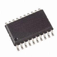
ATA5743P3-TGQY
Manufacturer Part Number
ATA5743P3-TGQY
Description
IC RCVR ASK/FSK 300KHZ 20SOIC
Manufacturer
Atmel
Datasheet
1.ATA5743P3-TGQY.pdf
(43 pages)
Specifications of ATA5743P3-TGQY
Frequency
300MHz ~ 450MHz
Sensitivity
-110dBm
Data Rate - Maximum
10 kBaud
Modulation Or Protocol
ASK, FSK
Applications
RKE, Telemetering, Security Technology
Current - Receiving
7.5mA
Data Interface
PCB, Surface Mount
Antenna Connector
PCB, Surface Mount
Voltage - Supply
4.5 V ~ 5.5 V
Operating Temperature
-40°C ~ 105°C
Package / Case
20-SOIC (0.300", 7.50mm Width)
Operating Frequency (max)
450000kHz
Operating Temperature (min)
-40C
Operating Temperature (max)
105C
Operating Temperature Classification
Industrial
Operating Supply Voltage (min)
4.5V
Operating Supply Voltage (typ)
5V
Operating Supply Voltage (max)
5.5V
Lead Free Status / RoHS Status
Lead free / RoHS Compliant
Features
-
Memory Size
-
Lead Free Status / Rohs Status
Compliant
Available stocks
Company
Part Number
Manufacturer
Quantity
Price
Company:
Part Number:
ATA5743P3-TGQY
Manufacturer:
ATMEL
Quantity:
203
Part Number:
ATA5743P3-TGQY
Manufacturer:
ATMEL/爱特梅尔
Quantity:
20 000
Table 6-10.
Note:
Table 6-11.
Note:
6.6.1
4839B–RKE–08/05
Lim_min5
Lim_max
...
...
...
...
0
0
0
0
1
1
1
5
0
0
0
1
1
1
1
1. Lim_min is also used to determine the margins of the data clock control logic (see section
1. Lim_max is also used to determine the margins of the data clock control logic (see section
Conservation of the Register Information
Lim_min4
Lim_max
Effect of the Configuration Word Lim_min
Effect of the Configuration Word Lim_max
Lim_min
Lim_max
...
...
0
0
0
1
1
1
1
...
...
4
0
0
0
0
1
1
1
(1)
(1)
Lim_min3
The ATA5743 has integrated power-on reset and brown-out detection circuitry to provide a
mechanism to preserve the RAM register information.
As seen in
drops below the threshold voltage V
configuration registers in that condition. Once V
minimum reset period t
turned on.
To indicate that condition, the receiver displays a reset marker (RM) at pin DATA after a reset.
The RM is represented by the fixed frequency f
a Low pulse t1 at pin DATA.
(Lim_min < 10 Is Not Applicable)
Lim_max
(Lim_max < 12 Is Not Applicable)
...
...
1
1
1
0
1
1
1
...
...
3
1
1
1
1
1
1
1
Figure 6-24 on page
Lim_min2
Lim_max
...
...
0
0
1
1
1
1
1
...
...
2
1
1
1
0
1
1
1
Rst
Lim_min1
. A POR is also generated when the supply voltage of the receiver is
Lim_max
...
...
1
1
0
0
0
1
1
...
...
1
0
0
1
0
0
1
1
28, a power-on reset (POR) is generated if the supply voltage V
Lim_min0
ThReset
Lim_max
...
...
0
1
0
1
1
0
1
...
...
0
0
1
0
1
1
0
1
. The default parameters are programmed into the
RM
S
exceeds V
USA: T
at a 50% duty-cycle. RM can be cancelled via
(T
Lim_max
Lim_min
(T
Lower Limit Value for Bit Check
Upper Limit Value for Bit Check
Lim_min
ThReset
Europe: T
= 342 µs, Europe: T
USA: T
(Lim_max - 1)
“Data Clock” on page
the POR is cancelled after the
Lim_min
“Data Clock” on page
21 (default)
41 (default)
Lim_max
Lim_max
10
11
12
61
62
63
12
13
14
61
62
63
= 652 µs,
= 662 µs)
Lim
ATA5743
Lim_min
XLim
T
Clk
19).
= 348 µs)
19).
)
T
Clk
)
27
S


