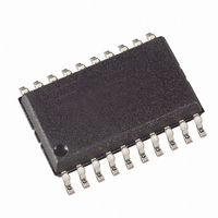
ATA5743P6-TGQY Atmel, ATA5743P6-TGQY Datasheet - Page 23

ATA5743P6-TGQY
Manufacturer Part Number
ATA5743P6-TGQY
Description
IC RCVR ASK/FSK 600KHZ 20SOIC
Manufacturer
Atmel
Datasheet
1.ATA5743P3-TGQY.pdf
(43 pages)
Specifications of ATA5743P6-TGQY
Frequency
300MHz ~ 450MHz
Sensitivity
-110dBm
Data Rate - Maximum
10 kBaud
Modulation Or Protocol
ASK, FSK
Applications
RKE, Telemetering, Security Technology
Current - Receiving
7.5mA
Data Interface
PCB, Surface Mount
Antenna Connector
PCB, Surface Mount
Voltage - Supply
4.5 V ~ 5.5 V
Operating Temperature
-40°C ~ 105°C
Package / Case
20-SOIC (0.300", 7.50mm Width)
Operating Frequency (max)
450000kHz
Operating Temperature (min)
-40C
Operating Temperature (max)
105C
Operating Temperature Classification
Industrial
Operating Supply Voltage (min)
4.5V
Operating Supply Voltage (typ)
5V
Operating Supply Voltage (max)
5.5V
Lead Free Status / RoHS Status
Lead free / RoHS Compliant
Features
-
Memory Size
-
Lead Free Status / Rohs Status
Compliant
Available stocks
Company
Part Number
Manufacturer
Quantity
Price
Company:
Part Number:
ATA5743P6-TGQY
Manufacturer:
ATMEL
Quantity:
222
Part Number:
ATA5743P6-TGQY
Manufacturer:
ATMEL/爱特梅尔
Quantity:
20 000
Figure 6-20. Output of Digital Noise at the End of the Data Stream
Figure 6-21. Automatic Noise Suppression
Figure 6-22. Occurrence of a Pulse at the End of the Data Stream
6.5.2
4839B–RKE–08/05
Controlled Noise Suppression by the Microcontroller
Data_out (DATA)
DATA_CLK
DATA_CLK
Data_out (DATA)
Dem_out
Data_out (DATA)
DATA_CLK
Bit-check
mode
Bit-check
mode
Bit check ok
Bit check ok
The controlled noise suppressionis illustrated in
(see
of a valid data stream. To suppress the noise, the pin POLLING/_ON must be set to Low. The
receiver remains in receiving mode. Then, the OFF command causes the change to the start-up
mode. The programmed sleep time (see
level at pin POLLING/_ON is Low, but the bit check is active. The OFF command activates the
bit check also if the pin POLLING/_ON is held to Low. The receiver changes back to receiving
mode if the bit check was successful. To activate the polling mode at the end of the data trans-
mission, the pin POLLING/_ON must be set to High.
This way of suppressing the noise is recommended if the data stream is not Manchester or
Bi-phase coded.
Preburst
Preburst
Receiving mode,
data clock control
logic active
Table 6-9 on page
Receiving mode,
data clock control
logic active
Receiving mode,
data clock control
logic active
1
Data stream
Timing error
Data
Data
1
1
26) in the OPMODE register is set to “0”, digital noise appears at the end
Digital Noise
(
T
ee
T
Receiving mode,
bit check aktive
ee
< T
Lim_min
Bit-check
mode
or T
T
Digital Noise
Pulse
Lim_max
Table 6-7 on page
Bit check ok
Bit check ok
< T
Digital noise
Figure 6-23 on page
ee
Preburst
Preburst
Bit-check mode
< T
Receiving mode,
data clock control
logic active
Receiving mode,
data clock control
logic active
Lim_min_2T
26) will not be executed because the
Data
Data
or T
ee
> T
24. If the bit Noise_Disable
Lim_max_2T
Receiving mode,
bit check aktive
Digital Noise
Bit-check
mode
)
ATA5743
23


