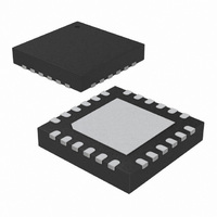
ATA5746-PXQW Atmel, ATA5746-PXQW Datasheet - Page 29

ATA5746-PXQW
Manufacturer Part Number
ATA5746-PXQW
Description
IC RCVR ASK/FSK UHF 24-QFN
Manufacturer
Atmel
Datasheet
1.ATA5745-EK.pdf
(44 pages)
Specifications of ATA5746-PXQW
Frequency
315MHz
Sensitivity
-114dBm
Data Rate - Maximum
10 kbps
Modulation Or Protocol
ASK, FSK
Applications
Alarm and Security Systems, RKE, TPMS
Current - Receiving
6.7mA
Data Interface
PCB, Surface Mount
Antenna Connector
PCB, Surface Mount
Voltage - Supply
2.7 V ~ 3.3 V, 4.5 V ~ 5.5 V
Operating Temperature
-40°C ~ 105°C
Package / Case
24-VQFN Exposed Pad, 24-HVQFN, 24-SQFN, 24-DHVQFN
Lead Free Status / RoHS Status
Lead free / RoHS Compliant
Features
-
Memory Size
-
Available stocks
Company
Part Number
Manufacturer
Quantity
Price
Company:
Part Number:
ATA5746-PXQW
Manufacturer:
ATMEL
Quantity:
3
11. Absolute Maximum Ratings
Stresses beyond those listed under “Absolute Maximum Ratings” may cause permanent damage to the device. This is a stress rating
only and functional operation of the device at these or any other conditions beyond those indicated in the operational sections of this
specification is not implied. Exposure to absolute maximum rating conditions for extended periods may affect device reliability.
12. Thermal Resistance
13. Electrical Characteristics: General
All parameters refer to GND and are valid for T
Typical values are given at V
consumption, timing, and digital pin properties can be found in the specific sections of the “Electrical Characteristics”.
4596B–RKE–06/07
*) Type means: A = 100% tested, B = 100% correlation tested, C = Characterized on samples, D = Design parameter
Note:
Parameters
Junction temperature
Storage temperature
Ambient temperature
Supply voltage VS5V
ESD (Human Body Model ESD S 5.1)
every pin
ESD (Machine Model JEDEC A115A)
every pin
ESD (Field Induced Charge Device Model ESD
STM 5.3.1-1999) every pin
Maximum input level, input matched to 50
Parameters
Junction ambient
No. Parameters
1.1
2.1
2.2
2.3 System start-up time
1
2
OFF Mode
Supply current in OFF
mode
Standby Mode
RF operating frequency
range
Supply current
Standby mode
1. Pin numbers in parenthesis were measured with RF_IN matched to 50 according to
nent values as in
VS3V_AVCC
Table 2-2 on page 6
Test Conditions
V
V
CLK_OUT disabled
ATA5746
ATA5745
XTO running
V
CLK_OUT disabled
XTO running
V
CLK_OUT disabled
XTO startup
XTAL: C
C
VS3V_AVCC
VS5V
VS3V_AVCC
VS5V
0
= 1.8 pF, R
= V
= 5V
= 5V
VS5V
m
= 5 fF,
= V
= V
amb
= 3V, T
m
VS5V
VS5V
= –40°C to +105°C, V
15
amb
(RF
3V
3V
Symbol
Symbol
= 25°C, and f
IN
FCDM
P
HBM
R
T
MM
T
in_max
).
V
T
amb
thJA
stg
S
j
10, 11
10,11
10,11
Pin
10
14
14
(1)
ATA5745/ATA5746 [Preliminary]
RF
VS3V_AVCC
T
= 315 MHz unless otherwise specified. Details about current
Symbol
XTO_Startup
I
I
Standby
Standby
I
SOFF
f
f
RF
RF
–200
–500
Min.
–55
–40
–4
= V
VS5V
Min.
313
433
= 2.7V to 3.3V, and V
Value
25
Figure 2-1 on page 6
Typ.
Max.
+150
+125
+105
+200
+500
0.3
50
50
+6
+4
0
VS5V
Max.
317
435
0.8
80
80
2
2
= 4.5V to 5.5V.
MHz
MHz
Unit
µA
µA
µA
µA
ms
with compo-
Unit
dBm
Unit
K/W
kV
°C
°C
°C
V
V
V
Type*
A
A
A
A
A
A
A
29


