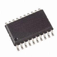
ATA5760N-TGSY Atmel, ATA5760N-TGSY Datasheet - Page 23

ATA5760N-TGSY
Manufacturer Part Number
ATA5760N-TGSY
Description
IC RCVR UHF ASKFSK 868MHZ 20SOIC
Manufacturer
Atmel
Datasheet
1.ATA5760N-TGSY.pdf
(41 pages)
Specifications of ATA5760N-TGSY
Frequency
868MHz
Sensitivity
-110dBm
Data Rate - Maximum
10 kBaud
Modulation Or Protocol
ASK, FSK
Applications
Telemetering and Security Systems
Current - Receiving
7.8mA
Data Interface
PCB, Surface Mount
Antenna Connector
PCB, Surface Mount
Voltage - Supply
4.5 V ~ 5.5 V
Operating Temperature
-40°C ~ 105°C
Package / Case
20-SOIC (0.300", 7.50mm Width)
Lead Free Status / RoHS Status
Lead free / RoHS Compliant
Features
-
Memory Size
-
11. Configuration of the Receiver
Table 11-3.
4896D–RKE–08/08
Bit 1
1
0
0
values of
Bit 3...14
values of
Bit 3...14
Default
Default
–
–
Bit 2
–
1
0
Effect of the Configuration Words within the Registers
Baud1
Bit 3
Lim_
min5
–
0
0
BR_Range
Baud0
Bit 4
Lim_
min4
–
0
1
The T5760/T5761 receiver is configured via two 12-bit RAM registers called OPMODE and
LIMIT. The registers can be programmed by means of the bidirectional DATA port. If the register
contents have changed due to a voltage drop, this condition is indicated by a certain output pat-
tern called reset marker (RM). The receiver must be reprogrammed in that case. After a
Power-On Reset (POR), the registers are set to default mode. If the receiver is operated in
default mode, there is no need to program the registers.
ture of the registers. According to
mode via the OFF command (see section
Bit 2 represents the register address. It selects the appropriate register to be programmed. To
get a high programming reliability, bit 15 (Stop bit), at the end of the programming operation,
must be set to 0.
Table 11-1.
Table 11-2.
Bit 1
BitChk1
1
0
0
Bit 5
Lim_
min3
–
0
0
Lim_min
N
Bit 15
Bit-check
0
1
Effect of Bit 1 and Bit 2 on Programming the Registers
Effect of Bit 15 on Programming the Register
BitChk0
Bit 6
Lim_
min2
–
1
1
Bit 2
x
1
0
Modu-lat
_FSK
ASK/
Bit 7
Lim_
min1
ion
–
0
0
Action
The receiver is set back to polling mode (OFF command)
The OPMODE register is programmed
The LIMIT register is programmed
Action
The values will be written into the register (OPMODE or LIMIT)
The values will not be written into the register
OFF command
OPMODE register
Sleep4
Bit 8
Lim_
min0
LIMIT register
–
0
1
Table
Sleep3
max5
Bit 9
Lim_
–
0
1
11-2, bit 1 defines if the receiver is set back to polling
“Receiving Mode” on page
Sleep2
Bit 10
max4
Lim_
Sleep
–
1
0
Sleep1
Bit 11
max3
Lim_
Table 11-3 on page 23
–
1
1
Lim_max
ATA5760/ATA5761
Sleep0 X
Bit 12
max2
Lim_
–
0
0
14) or if it is programmed.
Bit 13
X
max1
SleepStd
Lim_
Sleep
–
0
0
Suppression
shows the struc-
Disable
Noise_
Bit 14
Noise
max0
Lim_
–
1
1
Bit 15
–
–
0
–
–
–
0
–
23


