TDA5200 Infineon Technologies, TDA5200 Datasheet
TDA5200
Specifications of TDA5200
TDA5200INTR
TDA5200XT
TDA5200XT
TDA5200XTINTR
TDA5200XTINTR
Available stocks


Related parts for TDA5200

TDA5200 Summary of contents
Page 1
ASK Single Conversion Receiver Version 3 Revision 3.0, 2010-12- ...
Page 2
... Infineon Technologies Office. Infineon Technologies components may be used in life-support devices or systems only with the express written approval of Infineon Technologies failure of such components can reasonably be expected to cause the failure of that life-support device or system or to affect the safety or effectiveness of that device or system. Life support devices or systems are intended to be implanted in the human body or to support and/or maintain and sustain and/or protect human life ...
Page 3
... More detailed information of LNA high gain mode and LNA low gain mode Trademarks of Infineon Technologies AG AURIX™, BlueMoon™, C166™, CanPAK™, CIPOS™, CIPURSE™, COMNEON™, EconoPACK™, CoolMOS™, CoolSET™, CORECONTROL™, CROSSAVE™, DAVE™, EasyPIM™, EconoBRIDGE™, EconoDUAL™, EconoPIM™ ...
Page 4
Table of Contents Table of Contents . . . . . . . . . . . . . . . . . . . . . . . . . . . . . . . . . . ...
Page 5
List of Figures Figure 1 PG-TSSOP- ...
Page 6
List of Tables Table 1 Pin Definition and Function . . . . . . . . . . . . . . . . . . . . . . . . . . . . . . . ...
Page 7
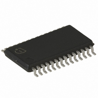
... Keyless Entry Systems • Remote Control Systems • Alarm Systems • Low Bitrate Communication Systems Package Figure 1 PG-TSSOP-28 Ordering Information Type TDA5200 1) Available on tape and reel Data Sheet I = 4.6 mA typ. at 434 MHz) s Ordering Code SP000016381 7 TDA 5200 ASK Single Conversion Receiver Product Info ...
Page 8
Product Description 2.1 Overview The very low power consumption single chip ASK Superheterodyne Receiver (SHR) for the frequency bands 868-870 MHz and 433-435 MHz. The IC offers a high level of integration and needs only a ...
Page 9
Package Outlines Figure 2 PG-TSSOP-28 Package Outlines Data Sheet ASK Single Conversion Receiver 9 Revision 3.0, 2010-12-28 TDA 5200 Product Description ...
Page 10
Functional Description 3.1 Pin Configuration CRST1 Figure 3 IC Pin Configuration Data Sheet 1 VCC 2 LNI 3 TAGC 4 AGND 5 LNO 6 VCC 7 TDA 5200 MI 8 MIX 9 AGND 10 FSEL 11 IFO 12 DGND ...
Page 11
Pin Definition and Function Table 1 Pin Definition and Function Pin Name Pin Buffer Type No. Type 1 CRST1 In/Out 2 VCC In 3 LNI In Data Sheet 4.15V 1 50uA 57uA ASK Single Conversion ...
Page 12
Table 1 Pin Definition and Function (cont’d) Pin Name Pin Buffer Type No. Type 4 TAGC In/Out 5 AGND In 6 LNO Out 7 VCC Data Sheet 4.3V 4.2uA 4 1k 1.5uA 1.7V 5V ...
Page 13
Table 1 Pin Definition and Function (cont’d) Pin Name Pin Buffer Type No. Type 9 MIX AGND In 11 FSEL In 12 IFO Out 12 13 DGND In 14 VDD In Data Sheet 400 uA 750 ...
Page 14
Table 1 Pin Definition and Function (cont’d) Pin Name Pin Buffer Type No. Type 15 LF In/Out 15 16 CSEL LIM Data Sheet ASK Single Conversion Receiver 5V 4.6V 30uA 200 100 30uA 2.4V ...
Page 15
Table 1 Pin Definition and Function (cont’d) Pin Name Pin Buffer Type No. Type 18 LIMX SLP SLN OPP In 21 Data Sheet ASK Single Conversion Receiver 2.4V 15k 75uA ...
Page 16
Table 1 Pin Definition and Function (cont’d) Pin Name Pin Buffer Type No. Type 22 FFB THRES 3VOUT Out 25 DATA Out 26 PDO Out Data Sheet 100k 10k 24 200 25 80k 200 ...
Page 17
Table 1 Pin Definition and Function (cont’d) Pin Name Pin Buffer Type No. Type 27 PDWN CRST2 In/Out Data Sheet 220k 220k 4.15V 28 50uA 17 TDA 5200 ASK Single Conversion Receiver Functional Description Function Power Down ...
Page 18
Functional Block Diagram V CC LNO LNA 4 TAGC 14 VDD DGND 13 2/7 5/10 VCC AGND Figure 4 Main Block Diagram Data Sheet IF Filter MI MIX IFO LIM LIMX ...
Page 19
Functional Blocks 3.4.1 Low Noise Amplifier (LNA) The LNA is an on-chip cascode amplifier with a voltage gain dB. The gain figure is determined by the external matching networks situated ahead of LNA and ...
Page 20
Crystal Oscillator The on-chip crystal oscillator circuitry allows for utilization of quartzes both in the 6 MHz and 13 MHz range as the overall division ratio of the PLL can be switched between 64 and 128 via the CSEL ...
Page 21
Table 4 PDWN Pin Operating States PDWN Open or tied to ground V Tied to CC Data Sheet ASK Single Conversion Receiver Operating State Power Down Mode Receiver On 21 TDA 5200 Functional Description Revision 3.0, 2010-12-28 ...
Page 22
Applications 4.1 Choice of LNA Threshold Voltage and Time Constant In the following figure the internal circuitry of the LNA automatic gain control is shown. Pins: RSSI > U threshold RSSI < U threshold Figure 5 LNA Automatic Gain ...
Page 23
Figure 6 Typical Curve of RSSI Level and Permissive AGC Threshold Levels The switching point should be chosen according to the intended operating scenario. The determination of the optimum point ...
Page 24
Data Filter Design Utilizing the on-board voltage follower and the two 100 kΩ on-chip resistors a 2 filter can be constructed by adding 2 external capacitors between pin 19 (SLP) and pin 22 (FFB) and to pin 21 (OPP) ...
Page 25
... MHz case and 15 pF and 8 the 13.401 MHz case. But please note that the calculated value of Data Sheet ASK Single Conversion Receiver C S Pin 28 Input impedance Z TDA5200 1-28 Pin 750 Ω 1250 Ω includes the parasitic capacitors also. ...
Page 26
Quartz Frequency Calculation As described in Chapter 3.4.3, the operating range of the on-chip VCO is 820 MHz to 860 MHz with a nominal center frequency of approximately 840 MHz. This signal is divided by 2 before applied to ...
Page 27
Data Slicer Threshold Generation The threshold of the data slicer can be generated in two ways, depending on the signal coding scheme used. In case of a signal coding scheme without DC content such as Manchester coding the threshold ...
Page 28
Electrical Characteristics 5.1 Electrical Data 5.1.1 Absolute Maximum Ratings Attention: The maximum ratings may not be exceeded under any circumstances, not even momentarily and individually, as permanent damage to the IC will result. Table 6 Absolute Maximum Ratings, Ambient ...
Page 29
Operating Range Within the operating range the IC operates as explained in the circuit description. The AC/DC characteristic limits are not guaranteed. V Supply voltage: = 4.5 V ... 5 Table 7 Operating Range, Ambient Temperature Parameter ...
Page 30
AC/DC Characteristics AC/DC characteristics involve the spread of values guaranteed within the specified voltage and ambient temperature range. Typical characteristics are the median of the production. The device performance parameters marked with ■ are not subject to production test. ...
Page 31
Table 8 AC/DC Characteristics with Parameter Symbol S Input impedance 11 LNA f = 868 MHz RF P1dB Input level @ LNA f = 434 MHz RF P1dB Input level @ LNA ...
Page 32
Table 8 AC/DC Characteristics with Parameter Symbol V LNA high gain mode THRES I Current in THRES_in AGC - Signal TAGC (PIN 4) I Current out, TAGC_out LNA low gain state I Current in, TAGC_in LNA high gain state MIXER ...
Page 33
Table 8 AC/DC Characteristics with Parameter Symbol C Capacitive loading of max SLIC output V LOW output voltage SLIC_L V HIGH output voltage SLIC_H I Output current SLIC_out PEAK DETECTOR - Signal Output PDO (PIN 26) V LOW output voltage ...
Page 34
Test Board 5.2.1 Test Circuit The device performance parameters marked with ■ in verified by design/characterization. Figure 11 Schematic of the Evaluation Board Data Sheet ASK Single Conversion Receiver Electrical Characteristics Chapter 5.1.3 are not subject to production test. ...
Page 35
Test Board Layouts Figure 12 Top Side of the Evaluation Board Figure 13 Bottom Side of the Evaluation Board Data Sheet ASK Single Conversion Receiver Electrical Characteristics 35 TDA 5200 Revision 3.0, 2010-12-28 ...
Page 36
Figure 14 Component Placement on the Evaluation Board Data Sheet ASK Single Conversion Receiver Electrical Characteristics 36 TDA 5200 Revision 3.0, 2010-12-28 ...
Page 37
... Bill of Materials The following components are necessary for evaluation of the TDA5200 without use of a Microchip HCS515 decoder. Table 9 Bill of Materials Ref Value R1 100 kΩ R2 100 kΩ R3 820 kΩ R4 120 kΩ R5 180 kΩ kΩ L1 434 MHz 868 MHz: 3 434 MHz: 8.2 pF 868 MHz: 3 ...
Page 38
Table 9 Bill of Materials Ref Value X1, X4, S1 IC1 TDA 5200 Please note that in case of operation at 434 MHz a capacitor has to be soldered in place of L2 and an inductor in place ...
Page 39
... Published by Infineon Technologies AG ...