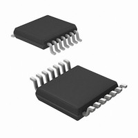
MRF49XA-I/ST Microchip Technology, MRF49XA-I/ST Datasheet - Page 11

MRF49XA-I/ST
Manufacturer Part Number
MRF49XA-I/ST
Description
IC RF TXRX 433/868/915 16-TSSOP
Manufacturer
Microchip Technology
Datasheet
1.MRF49XA-IST.pdf
(102 pages)
Specifications of MRF49XA-I/ST
Package / Case
16-TSSOP
Frequency
433MHz, 868MHz, 915MHz
Data Rate - Maximum
256kbps
Modulation Or Protocol
FHSS, FSK
Applications
Home / Industrial Automation, Remote Access, Security Alarms
Power - Output
7dbm
Sensitivity
-110dBm
Voltage - Supply
2.2 V ~ 3.8 V
Current - Receiving
11mA
Current - Transmitting
15mA
Data Interface
PCB, Surface Mount
Antenna Connector
PCB, Surface Mount
Operating Temperature
-40°C ~ 85°C
Number Of Receivers
1
Number Of Transmitters
2
Wireless Frequency
433 MHz to 915 MHz
Output Power
+ 7 dBm
Operating Supply Voltage
2.5 V, 3.3 V
Maximum Operating Temperature
+ 85 C
Mounting Style
SMD/SMT
Minimum Operating Temperature
- 40 C
Modulation
FHSS, FSK
Lead Free Status / RoHS Status
Lead free / RoHS Compliant
Memory Size
-
Lead Free Status / Rohs Status
Lead free / RoHS Compliant
Other names
579-MRF49XA-1/ST
Available stocks
Company
Part Number
Manufacturer
Quantity
Price
Company:
Part Number:
MRF49XA-I/ST
Manufacturer:
IR
Quantity:
450
Part Number:
MRF49XA-I/ST
Manufacturer:
MICROCHIP/微芯
Quantity:
20 000
TABLE 2-1:
© 2009 Microchip Technology Inc.
Pin
1
2
3
4
5
6
7
8
RCLKOUT/FCAP/
FSK/DATA/FSEL
CLKOUT
PIN DESCRIPTION
Symbol
FINT
SDO
SCK
IRO
SDI
CS
Digital Input/Output Frequency Shift Keying: Transmit FSK data input (with
Digital Input/Output Recovery Clock Output: Provides the clock recovered from
Digital Output
Digital Output
Digital Output
Digital Input
Digital Input
Digital Input
Type
Preliminary
Serial data input interface to MRF49XA (SPI input signal).
Serial clock interface (SPI clock).
Serial interface chip select (SPI chip/device select).
Serial data output interface from MRF49XA (SPI output
signal).
Interrupt Request Output: Receiver generates an
active-low interrupt request for the microcontroller on the
following events:
• The TXBREG (see Table 2-4) is ready to receive the
• The RXFIFOREG (see Table 2-4) has received the
• RXFIFOREG overflow/TXBREG underrun.
• Negative pulse on interrupt input pin (INT).
• Wake-up timer time-out.
• Supply voltage below the preprogrammed value is
• Power-on Reset (POR).
internal pull-up resistor of 133 kΩ).
Data: When configured as DATA, this pin functions as
follows:
• Data In: Manually modulates the data from the external
• Data Out: Receives data in conjunction with RCLKOUT
FIFO Select: Selects the FIFO and the first bit appears on
the next clock when reading the RXFIFOREG. The FSEL pin
has an internal pull-up resistor. This pin must be “high” when
the TX register is enabled. In order to achieve minimum
current consumption, keep this pin “high” in Sleep mode.
the incoming data if:
• FTYPE bit of BBFCREG (see Table 2-5) is configured as
• FIFO is disabled by configuring FIFOEN bit of
Filter Capacitor: This pin is a raw baseband data if the
FTYPE bit of BBFCREG is configured as a configuration
filter. The pin can be used by the host microcontroller for data
recovery.
FIFO Interrupt: When the internal FIFO, FIFOEN bit of
GENCREG is enabled, this pin acts as a FIFO full interrupt,
indicating that the FIFO has been filled to its preprogrammed
limit (see FFBC<3:0> bits in FIFORSTREG in Table 2-5).
Clock Output: The transceiver’s clock output can be used by
the host microcontroller as a clock source.
next byte.
preprogrammed amount of bits.
detected.
host microcontroller when the internal TXBREG is dis-
abled. If the TXBREG is enabled, this pin can be tied
“high” or left unconnected. When reading the internal
RXFIFOREG, this pin must be pulled “low”.
when the internal FIFO is not used.
digital filter and
GENCREG (see Table 2-5)
Description
MRF49XA
DS70590B-page 9


