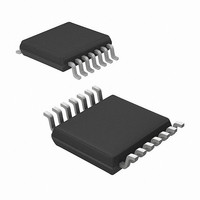
MRF49XA-I/ST Microchip Technology, MRF49XA-I/ST Datasheet - Page 13

MRF49XA-I/ST
Manufacturer Part Number
MRF49XA-I/ST
Description
IC RF TXRX 433/868/915 16-TSSOP
Manufacturer
Microchip Technology
Datasheet
1.MRF49XA-IST.pdf
(102 pages)
Specifications of MRF49XA-I/ST
Package / Case
16-TSSOP
Frequency
433MHz, 868MHz, 915MHz
Data Rate - Maximum
256kbps
Modulation Or Protocol
FHSS, FSK
Applications
Home / Industrial Automation, Remote Access, Security Alarms
Power - Output
7dbm
Sensitivity
-110dBm
Voltage - Supply
2.2 V ~ 3.8 V
Current - Receiving
11mA
Current - Transmitting
15mA
Data Interface
PCB, Surface Mount
Antenna Connector
PCB, Surface Mount
Operating Temperature
-40°C ~ 85°C
Number Of Receivers
1
Number Of Transmitters
2
Wireless Frequency
433 MHz to 915 MHz
Output Power
+ 7 dBm
Operating Supply Voltage
2.5 V, 3.3 V
Maximum Operating Temperature
+ 85 C
Mounting Style
SMD/SMT
Minimum Operating Temperature
- 40 C
Modulation
FHSS, FSK
Lead Free Status / RoHS Status
Lead free / RoHS Compliant
Memory Size
-
Lead Free Status / Rohs Status
Lead free / RoHS Compliant
Other names
579-MRF49XA-1/ST
Available stocks
Company
Part Number
Manufacturer
Quantity
Price
Company:
Part Number:
MRF49XA-I/ST
Manufacturer:
IR
Quantity:
450
Part Number:
MRF49XA-I/ST
Manufacturer:
MICROCHIP/微芯
Quantity:
20 000
2.1
The power supply bypassing is very essential for better
handling of signal surges and noise in the power line.
The large value decoupling capacitors should be
placed at the PCB power input. The smaller value
decoupling capacitors should be placed at every power
point of the device and at bias points for the RF port.
Poor bypassing leads to conducted interference which
can cause noise and spurious signals to couple into the
RF sections, thereby significantly reducing the
performance.
The V
sufficient bypass and decoupling. However, based on
the selected carrier frequency, the bypass capacitor
values vary. The recommended bypass capacitor
values are listed in Table 2-2 and the type of capacitor
to be used is listed in Table 2-3. The bypass capacitors
are connected to pin 14, as shown in Figure 4-1. The
trace length (V
made as short as possible.
TABLE 2-2:
TABLE 2-3:
2.2
An external hardware Reset of MRF49XA can be per-
formed by asserting the RESET (pin 10) to low. After
releasing the pin, it takes slightly more than 0.25 ms for
the transceiver to be released from the Reset. The pin
is driven with an open-drain output, and hence, it is
pulled down while the device is in POR. The RESET
pin has an internal, weak, on-chip, pull-up resistor. The
device will not accept commands during the Reset
period.
© 2009 Microchip Technology Inc.
SMD Size
Property
Dielectric
(MHz)
Band
433
868
915
DD
Power and Ground Pins
RESET Pin
pin requires two bypass capacitors to ensure
DD
Tantalum
C1(μF)
RECOMMENDED BYPASS
CAPACITORS VALUE
RECOMMENDED BYPASS
CAPACITORS
pin to bypass capacitors) should be
2.2
2.2
2.2
C1
A
Ceramic
C2 (nF)
0603
C2
10
10
10
Ceramic
C3 (pF)
0603
220
C3
47
33
Preliminary
The device enters the Reset mode if any of the
following events take place:
• Power-on Reset
• Power Glitch Reset
• Software Reset
• RESET Pin
Software Reset can be issued by sending the appropri-
ate control command to the device. The result of the
command is similar to POR, but the duration of the
Reset event is much less, typically 0.25 ms. The Soft-
ware Reset works only when the Sensitive Reset mode
is selected. See Section 3.1 “Reset” for details on
Reset; for connection details, see Figure 4-1.
2.3
The Power Amplifier (PA) has an open-collector differen-
tial output and can directly drive different PCB antennas,
like loop or dipole, with a programmable output power
level during signal transmission. However, certain types
of antennas, like monopole, need an additional matching
circuitry. A built-in, automatic antenna tuning circuit is
used to avoid the manual tuning and trimming
procedures during production process; the so called
“hand effect”.
2.4
The Low Noise Amplifier (LNA) has approximately
250Ω of differential input impedance which functions
well with the proposed antenna (PCB/Monopole) dur-
ing signal transmission. The LNA, when connected to
the 50Ω device, needs an external matching circuit
(Balun) for correct matching and to minimize the noise
figure of the receiver.
The LNA gain can be selected in four steps for different
gain factors (between 0 and -20 dB relative to the high-
est gain) based on the required RF signal strength.
This gain selection feature is useful in a noisy
environment.
Power Amplifier
Low Noise Amplifier
MRF49XA
DS70590B-page 11


