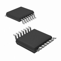
MRF49XA-I/ST Microchip Technology, MRF49XA-I/ST Datasheet - Page 17

MRF49XA-I/ST
Manufacturer Part Number
MRF49XA-I/ST
Description
IC RF TXRX 433/868/915 16-TSSOP
Manufacturer
Microchip Technology
Datasheet
1.MRF49XA-IST.pdf
(102 pages)
Specifications of MRF49XA-I/ST
Package / Case
16-TSSOP
Frequency
433MHz, 868MHz, 915MHz
Data Rate - Maximum
256kbps
Modulation Or Protocol
FHSS, FSK
Applications
Home / Industrial Automation, Remote Access, Security Alarms
Power - Output
7dbm
Sensitivity
-110dBm
Voltage - Supply
2.2 V ~ 3.8 V
Current - Receiving
11mA
Current - Transmitting
15mA
Data Interface
PCB, Surface Mount
Antenna Connector
PCB, Surface Mount
Operating Temperature
-40°C ~ 85°C
Number Of Receivers
1
Number Of Transmitters
2
Wireless Frequency
433 MHz to 915 MHz
Output Power
+ 7 dBm
Operating Supply Voltage
2.5 V, 3.3 V
Maximum Operating Temperature
+ 85 C
Mounting Style
SMD/SMT
Minimum Operating Temperature
- 40 C
Modulation
FHSS, FSK
Lead Free Status / RoHS Status
Lead free / RoHS Compliant
Memory Size
-
Lead Free Status / Rohs Status
Lead free / RoHS Compliant
Other names
579-MRF49XA-1/ST
Available stocks
Company
Part Number
Manufacturer
Quantity
Price
Company:
Part Number:
MRF49XA-I/ST
Manufacturer:
IR
Quantity:
450
Part Number:
MRF49XA-I/ST
Manufacturer:
MICROCHIP/微芯
Quantity:
20 000
2.14
The received data in MRF49XA is filled into a 16-bit
FIFO register. The FIFO is configured to generate an
interrupt after receiving a defined number of bits. When
the internal FIFO is enabled, the FIFO interrupt pin
(RCLKOUT/FCAP/FINT) acts as a FIFO full interrupt,
indicating that the FIFO has been filled to its prepro-
grammed limit. The receiver starts filling FIFO with data
when it identifies the synchronous pattern through the
synchronous pattern recognition circuit. During this
process, the FINTDIO bit changes its state. The FIFO
interrupt level is programmable from 1 to 16 bits. It is
recommended to set the threshold to at least half the
length of the register (8 bits) to ensure that the external
host microcontroller has time to set up. The synchronous
pattern recognition circuit prevents the FIFO from being
filled up with noise, and hence, avoids overloading the
external host microcontroller.
The FIFO read clock (SCK) must be < f
< 2.5 MHz
FSK/DATA/FSEL as the FIFO select pin, selects the
FIFO and the first bit appears on the next clock when
reading the RXFIFOREG.
In hardware, the FSK/DATA/FSEL pin is configured as
DATA (Data In) and with internal TXBREG disabled;
this manually modulates the data from the external host
microcontroller. If the TXBREG is enabled, this pin can
be tied “high” or can be left unconnected.
The internal synchronous pattern and the pattern
length are user-programmable. If the Chip Select (CS)
pin is low, the data bits on the SDI pin are shifted into
the device on the rising edge of the clock on the SCK
pin.The serial interface is initialized if the CS signal is
high.
© 2009 Microchip Technology Inc.
Note:
Receive FIFO
The synchronous word is not accessible in
the RX FIFO. The SYNBREG provides
this information to the host microcontroller.
for
10
MHz
on
RFXTAL.
XTAL
/4 or
The
Preliminary
2.15
The MRF49XA communicates with the host micro-
controller via a 4-wire SPI port as a slave device. An SPI
compatible serial interface lets the user select, com-
mand and monitor the status of the MRF49XA through
the host microcontroller. All registers consist of a com-
mand code, followed by a varying number of parameter
or data bits. As the device uses word writes, the CS pin
should be pulled low for 16 bits. Data bits on the SDI pin
are shifted into the device upon the rising edge of the
clock on the SCK pin whenever the CS pin is low.
The maximum clock frequency for the SPI bus is
20 MHz. The MRF49XA supports SPI Mode 0,0 which
requires the SCK to remain Idle in a low state. The CS
pin must be held low to enable communication between
the host microcontroller and the MRF49XA. The
device’s timing specification details are given in
Table 5-8. Data is received by the transceiver via the
SDI pin and is clocked on the rising edge of SCK. The
timing diagram is shown in Figure 5-1. MRF49XA
sends out the data via the SDO pin and is clocked out
on the falling edge of SCK. The Most Significant
bit (MSb) is sent first (e.g., bit 15 for a 16-bit command)
in any data. The POR circuit sets default values in all
control and command registers.
The SDO pin defaults to a low state when the CS pin is
high (the MRF49XA is not selected). This pin has a
tri-state buffer and uses a bus hold logic. For the SPI
interface, see Figure 4-1.
The following parameters can be programmed and set
through SPI:
• Frequency band
• Center frequency of the synthesizer
• Division ratio for the microcontroller clock
• Wake-up timer period
• Bandwidth of the baseband signal path
• Low supply voltage detector threshold
Any of these auxiliary functions can be disabled when
not required. After power-on, all parameters are set to
default values. The programmed values are retained
during Sleep mode. The interface supports the read out
of a status register which provides detailed information
about the status of the transceiver and the received
data.
Note:
Serial Peripheral Interface
interface should be implemented.
Special care must be taken when the micro-
controller’s built-in hardware serial port is
used. If the port cannot be switched to a
16-bit mode, then a separate I/O line should
be used to control the CS pin to ensure a
low level during the complete duration of the
command or a software serial control
MRF49XA
DS70590B-page 15


