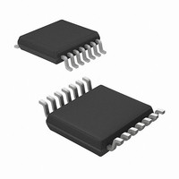
MRF49XA-I/ST Microchip Technology, MRF49XA-I/ST Datasheet - Page 18

MRF49XA-I/ST
Manufacturer Part Number
MRF49XA-I/ST
Description
IC RF TXRX 433/868/915 16-TSSOP
Manufacturer
Microchip Technology
Datasheet
1.MRF49XA-IST.pdf
(102 pages)
Specifications of MRF49XA-I/ST
Package / Case
16-TSSOP
Frequency
433MHz, 868MHz, 915MHz
Data Rate - Maximum
256kbps
Modulation Or Protocol
FHSS, FSK
Applications
Home / Industrial Automation, Remote Access, Security Alarms
Power - Output
7dbm
Sensitivity
-110dBm
Voltage - Supply
2.2 V ~ 3.8 V
Current - Receiving
11mA
Current - Transmitting
15mA
Data Interface
PCB, Surface Mount
Antenna Connector
PCB, Surface Mount
Operating Temperature
-40°C ~ 85°C
Number Of Receivers
1
Number Of Transmitters
2
Wireless Frequency
433 MHz to 915 MHz
Output Power
+ 7 dBm
Operating Supply Voltage
2.5 V, 3.3 V
Maximum Operating Temperature
+ 85 C
Mounting Style
SMD/SMT
Minimum Operating Temperature
- 40 C
Modulation
FHSS, FSK
Lead Free Status / RoHS Status
Lead free / RoHS Compliant
Memory Size
-
Lead Free Status / Rohs Status
Lead free / RoHS Compliant
Other names
579-MRF49XA-1/ST
Available stocks
Company
Part Number
Manufacturer
Quantity
Price
Company:
Part Number:
MRF49XA-I/ST
Manufacturer:
IR
Quantity:
450
Part Number:
MRF49XA-I/ST
Manufacturer:
MICROCHIP/微芯
Quantity:
20 000
2.16
The memory in MRF49XA is implemented as static
RAM and is accessible via the SPI port. Each memory
location functionally addresses a register, control,
status or data/FIFO fields, as shown in Table 2-5. The
command/control registers provide control, status and
device address for transceiver operations. The FIFOs
serve as temporary buffers for data transmission and
reception.
The commands to the device are sent serially. All
17 commands basically address the 17 registers
affiliated to it. The registers consist of a command
code, followed by control, data, status or parameter
bits. The MSb is sent first in all of the commands (e.g.,
bit 15 for a 16-bit command). The POR circuit sets the
default values in all control and command registers.
TABLE 2-4:
DS70590B-page 16
MRF49XA
SI. No. Register Name
10
11
12
13
14
15
16
17
1
2
3
4
5
6
7
8
9
Memory Organization
FIFORSTREG
RXFIFOREG
GENCREG
AFCCREG
BBFCREG
SYNBREG
PLLCREG
RXCREG
DRSREG
PMCREG
WTSREG
DCSREG
TXCREG
CFSREG
BCSREG
STSREG
TXBREG
CONTROL (COMMAND) REGISTER DESCRIPTION
Status Read Register
General Configuration Register
Automatic Frequency Control Configuration
Register
Transmit Configuration Register
Transmit Byte Register
Center Frequency Value Set Register
Receive Control Register
Baseband Filter Configuration Register
Receiver FIFO Read Register
FIFO and Reset Mode Configuration
Register
Synchronous Byte Configuration Register
Data Rate Value Set Register
Power Management Configuration Register
Wake-up Timer Value Set Register
Duty Cycle Value Set Register
Battery Threshold Detect and Clock Output
Value Set Register
PLL Configuration Register
Register Description
Preliminary
Note:
Receive register/FIFO, transmit register,
interrupt, frequency control and signal
strength, POR, wake-up timer, low battery
detect, data quality, clock recovery
Frequency band select, enables TX and RX
registers, crystal load capacitor bank value
AFC locking range, mode, accuracy and
enable
Modulation polarity, modulation bandwidth,
transmit power and deviation
Transmit data byte
Transmit or receive frequency
Function of pin 16, Data Indicator Output
mode, RX baseband bandwidth, low noise
amplifier gain, digital RSSI threshold
Clock Recovery mode, data indicator
parameter value and filter type
Receive data byte
FIFO interrupt level, FIFO start control and
FIFO enable, POR Sensitivity mode,
synchronous character length
Synchronous character pattern
Data rate prescalar set
Enables receive and transmit chain, base-
band circuit, synthesizer circuit, oscillator,
wake-up timer, low battery detect and clock
out
Wake-up timer values for time interval
Duty Cycle mode and value
Low battery detect threshold values and
clock output frequency
Clock out buffer speed, PLL bandwidth,
dithering and delay
Special care must be taken when the
microcontroller’s built-in hardware serial
port is used. If the port cannot be switched
to 16-bit mode, then a separate I/O line
should be used to control the CS pin to
ensure a low level during communication
with the host microcontroller.
Related Control Functions
© 2009 Microchip Technology Inc.


