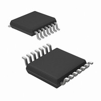
MRF49XA-I/ST Microchip Technology, MRF49XA-I/ST Datasheet - Page 23

MRF49XA-I/ST
Manufacturer Part Number
MRF49XA-I/ST
Description
IC RF TXRX 433/868/915 16-TSSOP
Manufacturer
Microchip Technology
Datasheet
1.MRF49XA-IST.pdf
(102 pages)
Specifications of MRF49XA-I/ST
Package / Case
16-TSSOP
Frequency
433MHz, 868MHz, 915MHz
Data Rate - Maximum
256kbps
Modulation Or Protocol
FHSS, FSK
Applications
Home / Industrial Automation, Remote Access, Security Alarms
Power - Output
7dbm
Sensitivity
-110dBm
Voltage - Supply
2.2 V ~ 3.8 V
Current - Receiving
11mA
Current - Transmitting
15mA
Data Interface
PCB, Surface Mount
Antenna Connector
PCB, Surface Mount
Operating Temperature
-40°C ~ 85°C
Number Of Receivers
1
Number Of Transmitters
2
Wireless Frequency
433 MHz to 915 MHz
Output Power
+ 7 dBm
Operating Supply Voltage
2.5 V, 3.3 V
Maximum Operating Temperature
+ 85 C
Mounting Style
SMD/SMT
Minimum Operating Temperature
- 40 C
Modulation
FHSS, FSK
Lead Free Status / RoHS Status
Lead free / RoHS Compliant
Memory Size
-
Lead Free Status / Rohs Status
Lead free / RoHS Compliant
Other names
579-MRF49XA-1/ST
Available stocks
Company
Part Number
Manufacturer
Quantity
Price
Company:
Part Number:
MRF49XA-I/ST
Manufacturer:
IR
Quantity:
450
Part Number:
MRF49XA-I/ST
Manufacturer:
MICROCHIP/微芯
Quantity:
20 000
REGISTER 2-3:
© 2009 Microchip Technology Inc.
bit 15
bit 7
Legend:
R = Readable bit
-n = Value at POR
bit 15-8
bit 7-6
bit 5-4
bit 3
bit 2
bit 1
Note 1:
R/W-1
R/W-1
2:
3:
AUTOMS<1:0>
The F
433 MHz = 2.5 kHz
868 MHz = 5 kHz
915 MHz = 7.5 kHz
The offset error value is stored in the Offset register (FOREN bit should be enabled) in the AFC block and
is added to the frequency control word of the PLL. Reset this bit before initiating another sample.
In High-Accuracy (Fine) mode, the processing time is twice the regular mode, but the uncertainty of the
measurement is significantly reduced.
CCB<15:8>: Command Code bits
The command code bits (11000100b) are serially sent to the microcontroller to identify the bits to be
written in the AFCCREG.
AUTOMS<1:0>: Automatic Mode Selection bits (for AFC)
These bits select the operation type (automatic/manual) for performing AFC based on the status of
the MFCS bit.
11 = Keeps offset independent for the state of the DIO signal
10 = Keeps offset only while receiving (DIO = High)
01 = Runs and measures only once after each power-up cycle
00 = Auto mode off (controlled by microcontroller)
ARFO<1:0>: Allowable Range for Frequency Offset bits
These bits select the offset range allowable between transmitter and receiver frequencies.
11 = +3 F
10 = +7 F
01 = +15 F
00 = No restriction
MFCS: Manual Frequency Control Strobe bit
This bit is the strobe signal which initiates the manual frequency control sample to calculate the offset error.
1 = A sample of a received signal is compared with a receiver Local Oscillator (LO) signal and an offset
0 = Ready for the next sample
HAM: High-Accuracy (Fine) Mode bit
1 = Switches the Frequency Control mode to High-Accuracy mode
0 = Frequency Control mode works in regular mode
FOREN: Frequency Offset Register Enable bit
1 = Enables the offset value calculated by the offset sample. The offset value is added to the
0 = Denies the addition of the offset value to the frequency control word of the PLL
RES
R/W-1
R/W-1
error is calculated. If bit 1 is enabled, the value is stored in the Offset register of the AFC block.
frequency control word of the PLL which tunes the desired carrier frequency.
is the frequency tuning resolution for each band. The F
AFCCREG: AUTOMATIC FREQUENCY CONTROL CONFIGURATION REGISTER
(POR: 0xC4F7)
RES
RES
RES
r = reserved bit
W = Writable bit
‘1’ = Bit is set
to -4 F
to -8 F
to -16 F
R/W-0
R/W-1
RES
RES
ARFO<1:0>
RES
(1)
R/W-0
R/W-1
Preliminary
CCB<15:8>
(3)
U = Unimplemented bit, read as ‘0’
‘0’ = Bit is cleared
R/W-0
R/W-0
MFCS
RES
R/W-1
R/W-1
HAM
for each band is as follows:
x = Bit is unknown
MRF49XA
FOREN
R/W-0
R/W-1
DS70590B-page 21
FOFEN
R/W-0
R/W-1
(2)
bit 8
bit 0


