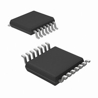
MRF49XA-I/ST Microchip Technology, MRF49XA-I/ST Datasheet - Page 34

MRF49XA-I/ST
Manufacturer Part Number
MRF49XA-I/ST
Description
IC RF TXRX 433/868/915 16-TSSOP
Manufacturer
Microchip Technology
Datasheet
1.MRF49XA-IST.pdf
(102 pages)
Specifications of MRF49XA-I/ST
Package / Case
16-TSSOP
Frequency
433MHz, 868MHz, 915MHz
Data Rate - Maximum
256kbps
Modulation Or Protocol
FHSS, FSK
Applications
Home / Industrial Automation, Remote Access, Security Alarms
Power - Output
7dbm
Sensitivity
-110dBm
Voltage - Supply
2.2 V ~ 3.8 V
Current - Receiving
11mA
Current - Transmitting
15mA
Data Interface
PCB, Surface Mount
Antenna Connector
PCB, Surface Mount
Operating Temperature
-40°C ~ 85°C
Number Of Receivers
1
Number Of Transmitters
2
Wireless Frequency
433 MHz to 915 MHz
Output Power
+ 7 dBm
Operating Supply Voltage
2.5 V, 3.3 V
Maximum Operating Temperature
+ 85 C
Mounting Style
SMD/SMT
Minimum Operating Temperature
- 40 C
Modulation
FHSS, FSK
Lead Free Status / RoHS Status
Lead free / RoHS Compliant
Memory Size
-
Lead Free Status / Rohs Status
Lead free / RoHS Compliant
Other names
579-MRF49XA-1/ST
Available stocks
Company
Part Number
Manufacturer
Quantity
Price
Company:
Part Number:
MRF49XA-I/ST
Manufacturer:
IR
Quantity:
450
Part Number:
MRF49XA-I/ST
Manufacturer:
MICROCHIP/微芯
Quantity:
20 000
REGISTER 2-10:
DS70590B-page 32
MRF49XA
bit 15
bit 7
Legend:
R = Readable bit
-n = Value at POR
bit 15-8
bit 7-4
bit 3
bit 2
bit 1
bit 0
Note 1:
R/W-1
R/W-1
2:
3:
On register overrun, the data will be lost. Therefore, the developer must take into account the processing
time required to read-out data before a register overrun. It is recommended to set the fill value to half of
the desired number of bits to be read to ensure sufficient time for additional processing. See Register 2-1
for the description of the TXRXFIFO and TXUROW bits, and Register 2-9 for details on polling and
interrupt driven FIFO reads from the SPI bus.
For synchronous character length selection, see Table 2-9.
For Reset mode selection, see Table 2-10.
CCB<15:8>: Command Code bits
The command code bits (11001010b) are serially sent to the microcontroller to identify the bits to be
written in the FIFORSTREG.
FFBC<3:0>: FIFO Fill Bit Count bits
Sets the received bits before generating an external interrupt to the host microcontroller to indicate the
receive FIFO is ready to be read. The maximum fill level is 15.
SYCHLEN: Synchronous Character Length bit
This bit sets the synchronous character length to byte or word long.
1 = Byte long. User-programmable SCL0 byte is used.
0 = Word long. The character is composed of the SCL1 and SCL0 bytes. The SCL1 byte value is fixed
FFSC: FIFO Fill Start Condition bit
This bit sets the condition at which the FIFO starts filling with data.
1 = The FIFO will continuously fill irrespective of noise or good data
0 = The FIFO will fill when it recognizes the synchronous character pattern as defined internally
FSCF: FIFO Synchronous Character Fill bit
1 = The FIFO starts filling with data when it detects the synchronous character pattern as defined in
0 = The FIFO fill stops
To restart the synchronous character pattern recognition, just clear and set this bit.
DRSTM: Disable (Sensitive) Reset Mode bit
1 = Disables
0 = Enables System Reset for any glitches above 0.2V in the power supply
R/W-1
R/W-0
and is not configurable. The SCL0 byte value is user-programmable through the SYNBREG.
the FFSC bit
FIFORSTREG: FIFO AND RESET MODE CONFIGURATION REGISTER
(POR: 0xCA80)
FFBC<3:0>
(3)
r = reserved bit
W = Writable bit
‘1’ = Bit is set
R/W-0
R/W-0
R/W-0
R/W-0
Preliminary
CCB<15:8>
U = Unimplemented bit, read as ‘0’
‘0’ = Bit is cleared
SYCHLEN
R/W-1
R/W-0
R/W-0
R/W-0
FFSC
(1)
(2)
© 2009 Microchip Technology Inc.
x = Bit is unknown
R/W-1
R/W-0
FSCF
(2)
DRSTM
R/W-0
R/W-0
bit 8
bit 0


