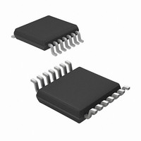
MRF49XA-I/ST Microchip Technology, MRF49XA-I/ST Datasheet - Page 38

MRF49XA-I/ST
Manufacturer Part Number
MRF49XA-I/ST
Description
IC RF TXRX 433/868/915 16-TSSOP
Manufacturer
Microchip Technology
Datasheet
1.MRF49XA-IST.pdf
(102 pages)
Specifications of MRF49XA-I/ST
Package / Case
16-TSSOP
Frequency
433MHz, 868MHz, 915MHz
Data Rate - Maximum
256kbps
Modulation Or Protocol
FHSS, FSK
Applications
Home / Industrial Automation, Remote Access, Security Alarms
Power - Output
7dbm
Sensitivity
-110dBm
Voltage - Supply
2.2 V ~ 3.8 V
Current - Receiving
11mA
Current - Transmitting
15mA
Data Interface
PCB, Surface Mount
Antenna Connector
PCB, Surface Mount
Operating Temperature
-40°C ~ 85°C
Number Of Receivers
1
Number Of Transmitters
2
Wireless Frequency
433 MHz to 915 MHz
Output Power
+ 7 dBm
Operating Supply Voltage
2.5 V, 3.3 V
Maximum Operating Temperature
+ 85 C
Mounting Style
SMD/SMT
Minimum Operating Temperature
- 40 C
Modulation
FHSS, FSK
Lead Free Status / RoHS Status
Lead free / RoHS Compliant
Memory Size
-
Lead Free Status / Rohs Status
Lead free / RoHS Compliant
Other names
579-MRF49XA-1/ST
Available stocks
Company
Part Number
Manufacturer
Quantity
Price
Company:
Part Number:
MRF49XA-I/ST
Manufacturer:
IR
Quantity:
450
Part Number:
MRF49XA-I/ST
Manufacturer:
MICROCHIP/微芯
Quantity:
20 000
REGISTER 2-13:
DS70590B-page 36
MRF49XA
bit 15
bit 7
Legend:
R = Readable bit
-n = Value at POR
bit 15-8
bit 7
bit 6
bit 5
bit 4
bit 3
bit 2
bit 1
Note 1:
RXCEN
R/W-1
R/W-0
2:
3:
4:
This bit can be disabled to reduce current consumption.
See BCSREG (Register 2-16) for programming details.
See WTSREG (Register 2-14) for details on programming the wake-up timer value.
If the CLKOEN bit is cleared by enabling the clock output, the oscillator continues to run even if the
OSCEN bit is cleared. The device will not fully enter into the Sleep mode.
CCB<15:8>: Command Code bits
The command code bits (10000010b) are serially sent to the microcontroller to identify the bits to be
written in the PMCREG.
RXCEN: Receiver Chain Enable bit
The receiver chain consists of a baseband circuit, synthesizer and crystal oscillator.
1 = Enables receiver chain
0 = Disables receiver chain
BBCEN: Baseband Circuit Enable bit
The baseband circuit, synthesizer and oscillator work together to demodulate and recover the data
transmitted to the synthesizer (SYNEN bit). The OSCEN bit must be enabled along with the baseband
circuits in order to receive data.
1 = Enables baseband circuit
0 = Disables baseband circuit
TXCEN: Transmit Chain Enable bit
The transmit chain consists of power amplifier, synthesizer, oscillator and transmit register.
1 = Enables the transmitter chain and starts transmission (if the TX register is enabled)
0 = Disables transmitter chain
SYNEN: Synthesizer Enable bit
The synthesizer consists of a PLL, oscillator and VCO for controlling the channel frequency.
1 = Enables the synthesizer
0 = Disables the synthesizer
OSCEN: Crystal Oscillator Enable bit
1 = Enables the crystal oscillator
0 = Disables the crystal oscillator
LBDEN: Low Battery Detector Enable bit
The battery detector can be programmed to 32 different threshold levels.
1 = Enables the battery voltage detector circuit
0 = Disables the battery voltage detector circuit
WUTEN: Wake-up Timer Enable bit
1 = Enables the wake-up timer circuit
0 = Disables the wake-up timer circuit
BBCEN
R/W-0
R/W-0
PMCREG: POWER MANAGEMENT CONFIGURATION REGISTER
(POR: 0x8208)
(1)
r = reserved bit
W = Writable bit
‘1’ = Bit is set
TXCEN
R/W-0
R/W-0
SYNEN
R/W-0
R/W-0
Preliminary
(3)
CCB<15:8>
(1)
U = Unimplemented bit, read as ‘0’
‘0’ = Bit is cleared
OSCEN
R/W-0
R/W-1
LBDEN
R/W-0
R/W-0
© 2009 Microchip Technology Inc.
(2)
x = Bit is unknown
WUTEN
R/W-1
R/W-0
(3)
CLKOEN
R/W-0
R/W-0
bit 8
bit 0


