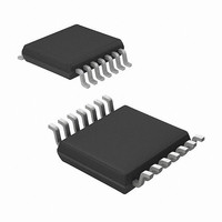
MRF49XA-I/ST Microchip Technology, MRF49XA-I/ST Datasheet - Page 54

MRF49XA-I/ST
Manufacturer Part Number
MRF49XA-I/ST
Description
IC RF TXRX 433/868/915 16-TSSOP
Manufacturer
Microchip Technology
Datasheet
1.MRF49XA-IST.pdf
(102 pages)
Specifications of MRF49XA-I/ST
Package / Case
16-TSSOP
Frequency
433MHz, 868MHz, 915MHz
Data Rate - Maximum
256kbps
Modulation Or Protocol
FHSS, FSK
Applications
Home / Industrial Automation, Remote Access, Security Alarms
Power - Output
7dbm
Sensitivity
-110dBm
Voltage - Supply
2.2 V ~ 3.8 V
Current - Receiving
11mA
Current - Transmitting
15mA
Data Interface
PCB, Surface Mount
Antenna Connector
PCB, Surface Mount
Operating Temperature
-40°C ~ 85°C
Number Of Receivers
1
Number Of Transmitters
2
Wireless Frequency
433 MHz to 915 MHz
Output Power
+ 7 dBm
Operating Supply Voltage
2.5 V, 3.3 V
Maximum Operating Temperature
+ 85 C
Mounting Style
SMD/SMT
Minimum Operating Temperature
- 40 C
Modulation
FHSS, FSK
Lead Free Status / RoHS Status
Lead free / RoHS Compliant
Memory Size
-
Lead Free Status / Rohs Status
Lead free / RoHS Compliant
Other names
579-MRF49XA-1/ST
Available stocks
Company
Part Number
Manufacturer
Quantity
Price
Company:
Part Number:
MRF49XA-I/ST
Manufacturer:
IR
Quantity:
450
Part Number:
MRF49XA-I/ST
Manufacturer:
MICROCHIP/微芯
Quantity:
20 000
3.9.1
The device’s interrupt pin (IRO) signals one of eight
interrupt events to the host microcontroller. The inter-
rupt source in the microcontroller is read out from the
transceiver through the SDO pin. The interrupt sources
that are available are briefly described in the following
subsections.
3.9.1.1
1.
2.
3.9.1.2
The POR interrupt is generated when a change on the
V
Reset was issued. For details, see Section 3.1
“Reset”.
3.9.1.3
1.
2.
DS70590B-page 52
MRF49XA
DD
Transmit mode: Transmit Register Ready bit
This interrupt is generated when the Transmit
register is empty. It is valid only when the
TXDEN bit (GENCREG<7>) is set and the
TXCEN bit (PMCREG<5>) is enabled.
Receive mode: Receive FIFO Empty bit
This interrupt is generated when the bit level in
the
programmed level. An interrupt is triggered when
the number of received data bits in the receiver
FIFO reaches the threshold set by the FFBC bits
(FIFORSTREG<7:4>). This is valid only when
the FIFOEN bit (GENCREG<6>) is set and the
RXCEN bit (PMCREG<7>) is enabled.
Transmit mode: Transmit Register Underrun or
Overwrite bit
This interrupt is generated when the automatic
Baud Rate Generator (BRG) has completed the
transmission of a byte in TXBREG before the
register
(GENCREG<7>) is set and the TXCEN bit
(PMCREG<5>) is enabled.
Receive mode: Receive FIFO Overflow bit
This interrupt is generated when the bits
received are more than the FIFO capacity
(16 bits). This is valid only when the FIFOEN bit
(GENCREG<6>) is set and the RXCEN bit
(PMCREG<7>) is enabled.
line triggers an internal Reset circuit or a Software
RXFIFOREG
SETTING INTERRUPTS
write.
TXRXFIFO: Transmit Register or
Receive FIFO bit
POR: Power-on Reset Interrupt
TXOWRXOF: Transmit Overwrite
Receive Overflow bit
It is valid only when the TXDEN bit
has
reached
the
pre-
Preliminary
3.9.1.4
This interrupt occurs when the time specified by the
wake-up timer has elapsed. It is valid only when the
WUTEN bit (PMCREG<1>) is set. The device periodi-
cally wakes up and switches to Receive mode. If valid
FSK data is received, the device sends an interrupt to
the microcontroller and continues filling the RXFIFO.
After the completion of transmission, the FIFO is read
out completely and all other interrupts are cleared. The
device returns to the Low-Power Consumption mode.
3.9.1.5
Follows the level of the INT pin if configured as an
external interrupt by clearing the FINTDIO bit
(RXCREG<10>).
3.9.1.6
This interrupt occurs when V
programmable low battery detector threshold level con-
figured by the LBDVB bits (BCSREG<3:0>). It is valid
only when the LBDEN bit (PMCREG<2>) is set.
3.9.2
If any of the interrupt sources gets active, the IRO
changes to logic low level and the corresponding
interrupt bit in the status byte goes high. Clearing an
interrupt implies:
• Releasing the IRO pin to return to logic high, and
• Clearing the corresponding interrupt bit in the
The clearing of each of the interrupts is briefly
described in the following subsections.
3.9.2.1
1.
2.
3.9.2.2
The IRO pin and its status bit are cleared by reading the
Status Read register.
STSREG
Transmit mode
The IRO pin and its status bit remain active until
the register is written (if underrun does not occur
until the register write) or the transmitter and the
TX latch are switched off.
Receive mode
The IRO pin and its status bit remain active until
the FIFO is read (receive FIFO interrupt thresh-
old number of bits have been read). The
receiver is switched off or the RXFIFO is
switched off.
CLEARING INTERRUPTS
WUTINT: Wake-up Timer Interrupt
LCEXINT: Logic Low-Level Change
on External Interrupt
LBTD: Low Battery Threshold Detect
TXRXFIFO
POR
© 2009 Microchip Technology Inc.
DD
goes below the


