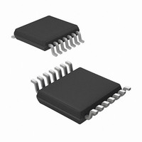
MRF49XA-I/ST Microchip Technology, MRF49XA-I/ST Datasheet - Page 65

MRF49XA-I/ST
Manufacturer Part Number
MRF49XA-I/ST
Description
IC RF TXRX 433/868/915 16-TSSOP
Manufacturer
Microchip Technology
Datasheet
1.MRF49XA-IST.pdf
(102 pages)
Specifications of MRF49XA-I/ST
Package / Case
16-TSSOP
Frequency
433MHz, 868MHz, 915MHz
Data Rate - Maximum
256kbps
Modulation Or Protocol
FHSS, FSK
Applications
Home / Industrial Automation, Remote Access, Security Alarms
Power - Output
7dbm
Sensitivity
-110dBm
Voltage - Supply
2.2 V ~ 3.8 V
Current - Receiving
11mA
Current - Transmitting
15mA
Data Interface
PCB, Surface Mount
Antenna Connector
PCB, Surface Mount
Operating Temperature
-40°C ~ 85°C
Number Of Receivers
1
Number Of Transmitters
2
Wireless Frequency
433 MHz to 915 MHz
Output Power
+ 7 dBm
Operating Supply Voltage
2.5 V, 3.3 V
Maximum Operating Temperature
+ 85 C
Mounting Style
SMD/SMT
Minimum Operating Temperature
- 40 C
Modulation
FHSS, FSK
Lead Free Status / RoHS Status
Lead free / RoHS Compliant
Memory Size
-
Lead Free Status / Rohs Status
Lead free / RoHS Compliant
Other names
579-MRF49XA-1/ST
Available stocks
Company
Part Number
Manufacturer
Quantity
Price
Company:
Part Number:
MRF49XA-I/ST
Manufacturer:
IR
Quantity:
450
Part Number:
MRF49XA-I/ST
Manufacturer:
MICROCHIP/微芯
Quantity:
20 000
3.16
The advanced interrupt handler circuit is configured in
the transmitter to reduce the power consumption. As
mentioned, the Sleep mode is the lowest power con-
sumption mode in which the clock and all functional
blocks of the device are disabled. In case of any inter-
rupt, the device wakes up, switches to Active mode and
an interrupt signal generated on the IRO pin indicates
the change in state to the host microcontroller. The
source of the interrupt can be determined by reading
the status word of the device (see Register 2-1).
To reduce current consumption, the MRF49XA should
be placed in the low-power consuming Sleep mode. In
Sleep mode, the 10 MHz main oscillator is turned off,
disabling the RF and baseband circuitry. Data is
retained in the control and FIFO registers and the
transceiver is accessible via the SPI port.
The MRF49XA will not enter Sleep mode if any of the
interrupt remains active, irrespective of the state of the
OSCEN bit in the PMCREG. This way, the micro-
controller can always have a clock signal to process the
interrupt. To prevent high-current consumption, which
results in shorter battery life, it is highly recommended
to process and clear interrupts before entering Sleep
mode. The functions which are not necessary should
be turned off to avoid unwanted interrupts.
To minimize the current consumption, the MRF49XA
supports different power-saving modes, along with an
integrated wake-up timer. Active mode can be
reinitiated by the following ways:
• By applying the wake-up events’ negative logical
• Wake-up timer time-out
• Low supply voltage detection
• On-chip FIFO filled up
• On receiving a request through the serial interface
To make the MRF49XA device enter into Sleep mode,
certain control register values must be initialized. The
sequence to program the control registers for entering
into Sleep and Wake-up modes is as follows:
For Sleep mode:
1.
2.
3.
4.
For Wake-up mode:
1.
2.
3.
© 2009 Microchip Technology Inc.
pulse on INT pin
Check the IRO bit status
Read STSREG
Configure GENCREG
Configure PMCREG for oscillator and clock
buffering
Enter in TX/RX mode or
Enable crystal or
Set the INT pin
Sleep, Wake-up and Battery
Operations
Preliminary
The device has the ability to wake itself up from Sleep
mode through a wake-up timer. The WTSREG sets the
wake-up interval for the MRF49XA. After setting the
wake-up interval, the WUTEN bit (PMCREG<1>)
should be cleared and set at the end of every wake-up
cycle.
The Wake-up Duration Time (WUTIME) is calculated
as shown in Equation 3-4.
EQUATION 3-4:
The Battery Threshold Detect feature is useful in
monitoring the discharge-sensitive batteries, such as
Lithium cells. The LBDEN bit (PMCREG<2>) is used to
enable or disable the low battery detect feature.
The BCSREG configures the following:
• Output clock frequency
• Low battery detect threshold
The low battery threshold value is programmable from
2.2V to 3.8V and is calculated by using Equation 3-5.
EQUATION 3-5:
When the battery level falls 50 mV below this value, the
LBTD bit (STSREG<10>) is set, indicating that the
battery level is below the programmed threshold.
The registers associated with power-saving modes
are:
• STSREG (see Register 2-1)
• GENCREG (see Register 2-2)
• TXCREG (see Register 2-4)
• RXCREG (see Register 2-7)
• PMCREG (see Register 2-13)
• WTSREG (see Register 2-14)
• BCSREG (see Register 2-16)
WUTIME = 1.03 x WTMV<7:0> x 2
where:
WTMV<7:0> = Decimal Value between 0 to 255
WTEV<4:0> = Decimal Value between 0 to 29
Note: WUTIME is measured in ms.
Threshold Voltage Value = 2.25 + 0.1 x (LBDVB<3:0>)
where:
LBDVB<3:0> is the Decimal Value from 0-15
MRF49XA
WTEV<4:0>
DS70590B-page 63
+ 0.5 ms


