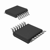
MRF49XA-I/ST Microchip Technology, MRF49XA-I/ST Datasheet - Page 66

MRF49XA-I/ST
Manufacturer Part Number
MRF49XA-I/ST
Description
IC RF TXRX 433/868/915 16-TSSOP
Manufacturer
Microchip Technology
Datasheet
1.MRF49XA-IST.pdf
(102 pages)
Specifications of MRF49XA-I/ST
Package / Case
16-TSSOP
Frequency
433MHz, 868MHz, 915MHz
Data Rate - Maximum
256kbps
Modulation Or Protocol
FHSS, FSK
Applications
Home / Industrial Automation, Remote Access, Security Alarms
Power - Output
7dbm
Sensitivity
-110dBm
Voltage - Supply
2.2 V ~ 3.8 V
Current - Receiving
11mA
Current - Transmitting
15mA
Data Interface
PCB, Surface Mount
Antenna Connector
PCB, Surface Mount
Operating Temperature
-40°C ~ 85°C
Number Of Receivers
1
Number Of Transmitters
2
Wireless Frequency
433 MHz to 915 MHz
Output Power
+ 7 dBm
Operating Supply Voltage
2.5 V, 3.3 V
Maximum Operating Temperature
+ 85 C
Mounting Style
SMD/SMT
Minimum Operating Temperature
- 40 C
Modulation
FHSS, FSK
Lead Free Status / RoHS Status
Lead free / RoHS Compliant
Memory Size
-
Lead Free Status / Rohs Status
Lead free / RoHS Compliant
Other names
579-MRF49XA-1/ST
Available stocks
Company
Part Number
Manufacturer
Quantity
Price
Company:
Part Number:
MRF49XA-I/ST
Manufacturer:
IR
Quantity:
450
Part Number:
MRF49XA-I/ST
Manufacturer:
MICROCHIP/微芯
Quantity:
20 000
3.17
In Data Transmission mode (enabled by the TXDEN bit
(GENCREG<7>)), the TX data is clocked into one of
the two 8-bit data registers. The transmitter starts to
send the data from the first register (with the given bit
rate) when the TXCEN bit (PMCREG<5>) is set. The
initial value of the data registers (0xAA) can be used to
generate preamble. During this mode, the SDO pin is
monitored to check whether the register is ready (SDO
is high) to receive the next byte from the micro-
controller. The block diagrams of the Transmit register,
before and during transmit, are shown in Figure 3-14
and Figure 3-15, respectively.
FIGURE 3-14:
DS70590B-page 64
MRF49XA
Serial Bus Data
TX Register Buffered Data
Transmission
(Register Initial Fill-up)
SCLK
TXCEN = 0
TX REGISTER BLOCK DIAGRAM (BEFORE TRANSMIT)
CLK
SDI
SDI
CLK
Preliminary
8-Bit Shift Register
8-Bit Shift Register
(Default: AAh)
(Default: AAh)
The transmitter FSK modulation parameters are used
for calculating the resulting output frequency, as shown
in Equation 3-6.
EQUATION 3-6:
f
where:
f
(see Register 2-6 for f
MB is the 4-bit Binary Number (MODBW<3:0>)
SIGN = MODPLY
FSKOUT
0
is the Channel Center Frequency
= f
0
+ (-1)SIGN x (MB + 1) x (15 kHz)
SDO
SDO
XOR
0
calculation)
© 2009 Microchip Technology Inc.
FSK
TX_DATA


