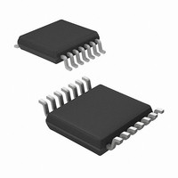
MRF49XA-I/ST Microchip Technology, MRF49XA-I/ST Datasheet - Page 71

MRF49XA-I/ST
Manufacturer Part Number
MRF49XA-I/ST
Description
IC RF TXRX 433/868/915 16-TSSOP
Manufacturer
Microchip Technology
Datasheet
1.MRF49XA-IST.pdf
(102 pages)
Specifications of MRF49XA-I/ST
Package / Case
16-TSSOP
Frequency
433MHz, 868MHz, 915MHz
Data Rate - Maximum
256kbps
Modulation Or Protocol
FHSS, FSK
Applications
Home / Industrial Automation, Remote Access, Security Alarms
Power - Output
7dbm
Sensitivity
-110dBm
Voltage - Supply
2.2 V ~ 3.8 V
Current - Receiving
11mA
Current - Transmitting
15mA
Data Interface
PCB, Surface Mount
Antenna Connector
PCB, Surface Mount
Operating Temperature
-40°C ~ 85°C
Number Of Receivers
1
Number Of Transmitters
2
Wireless Frequency
433 MHz to 915 MHz
Output Power
+ 7 dBm
Operating Supply Voltage
2.5 V, 3.3 V
Maximum Operating Temperature
+ 85 C
Mounting Style
SMD/SMT
Minimum Operating Temperature
- 40 C
Modulation
FHSS, FSK
Lead Free Status / RoHS Status
Lead free / RoHS Compliant
Memory Size
-
Lead Free Status / Rohs Status
Lead free / RoHS Compliant
Other names
579-MRF49XA-1/ST
Available stocks
Company
Part Number
Manufacturer
Quantity
Price
Company:
Part Number:
MRF49XA-I/ST
Manufacturer:
IR
Quantity:
450
Part Number:
MRF49XA-I/ST
Manufacturer:
MICROCHIP/微芯
Quantity:
20 000
3.18.1
The user can define the FIFO interrupt level (the num-
ber of received bits) which generates the FINT when
the level is exceeded. In this case, the Status bits report
the changed FIFO status.
TABLE 3-4:
FIGURE 3-19:
© 2009 Microchip Technology Inc.
Receive
Note:
Mode
INTERRUPT MODE
During FIFO access, f
higher than f
oscillator frequency. If the duty cycle of the
clock signal is not 50%, the shorter period
of the clock pulse should be at least 2/f
FSEL
SDO
FINT
SCK
CS
FIFOEN = 0
FIFOEN = 1
Bit Setting
RECEIVE PIN FUNCTION
FIFO READ EXAMPLE WITH FINT POLLING
ref
/4, where f
FIFO OUT
Receiver FIFO Disabled
Receiver FIFO Enabled
SCK
ref
is the crystal
Function
cannot be
0
VS
FO + 1
ref
Preliminary
. OPERATION MODE
1
.
FIFO Read Out
FO + 2
2
3.18.2
When the FSEL signal is low, the FIFO output is con-
nected directly to the SDO pin and its contents are
clocked out by the SCK pin. Set the FIFO interrupt level
to 1. In this case, as long as FINT indicates received
bits in the FIFO, the microcontroller continues to take
the bits away. When FINT goes low, no more bits need
to be taken.
An SPI read command (Receiver FIFO Read Com-
mand) is also available to read out the contents of the
FIFO. See Figure 3-19 for a simple receiver FIFO read,
in Polling mode, on SPI lines.
The registers associated with reception are:
• STSREG (see Register 2-1)
• GENCREG (see Register 2-2)
• RXCREG (see Register 2-7)
• FIFORSTREG (see Register 2-10)
• PMCREG (see Register 2-13)
(RX data FIFO can be
FO + 3
RX Data Output
3
FSEL Input
accessed)
Pin 6
POLLING MODE
4
FO + 4
MRF49XA
RX Data Clock Output
FINT Output
DS70590B-page 69
Pin 7


