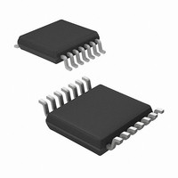
MRF49XA-I/ST Microchip Technology, MRF49XA-I/ST Datasheet - Page 74

MRF49XA-I/ST
Manufacturer Part Number
MRF49XA-I/ST
Description
IC RF TXRX 433/868/915 16-TSSOP
Manufacturer
Microchip Technology
Datasheet
1.MRF49XA-IST.pdf
(102 pages)
Specifications of MRF49XA-I/ST
Package / Case
16-TSSOP
Frequency
433MHz, 868MHz, 915MHz
Data Rate - Maximum
256kbps
Modulation Or Protocol
FHSS, FSK
Applications
Home / Industrial Automation, Remote Access, Security Alarms
Power - Output
7dbm
Sensitivity
-110dBm
Voltage - Supply
2.2 V ~ 3.8 V
Current - Receiving
11mA
Current - Transmitting
15mA
Data Interface
PCB, Surface Mount
Antenna Connector
PCB, Surface Mount
Operating Temperature
-40°C ~ 85°C
Number Of Receivers
1
Number Of Transmitters
2
Wireless Frequency
433 MHz to 915 MHz
Output Power
+ 7 dBm
Operating Supply Voltage
2.5 V, 3.3 V
Maximum Operating Temperature
+ 85 C
Mounting Style
SMD/SMT
Minimum Operating Temperature
- 40 C
Modulation
FHSS, FSK
Lead Free Status / RoHS Status
Lead free / RoHS Compliant
Memory Size
-
Lead Free Status / Rohs Status
Lead free / RoHS Compliant
Other names
579-MRF49XA-1/ST
Available stocks
Company
Part Number
Manufacturer
Quantity
Price
Company:
Part Number:
MRF49XA-I/ST
Manufacturer:
IR
Quantity:
450
Part Number:
MRF49XA-I/ST
Manufacturer:
MICROCHIP/微芯
Quantity:
20 000
4.2
The MRF49XA is designed to drive a differential output,
such as a dipole antenna or a loop antenna. The loop
antenna is ideally suited for applications where com-
pact size is required. The dipole is typically not a good
option for compact designs due to its inherent size at
resonance, and its space requirements around the
ground plane, to be an efficient antenna. A monopole
antenna can be used, along with a balun, or by using
the matching circuit.
TABLE 4-1:
4.4
The guidelines in this section help the users in
high-frequency PCB layout design.
The printed circuit board is usually comprised of two or
four basic FR4 layers.
The two-layer printed circuit board has mixed
signal/power/RF and common ground routed in both
the layers.
FIGURE 4-3:
FIGURE 4-4:
DS70590B-page 72
MRF49XA
Antenna Design Considerations
General PCB Layout Design
MRF49XA
433 MHz
868 MHz
915 MHz
FREQUENCY BAND – ANTENNA ADMITTANCE/IMPEDANCE
TWO BASIC COPPER FR4 LAYERS
FOUR BASIC COPPER FR4 LAYERS
Admittance (ms)
1.49-j12.8
1.2-j11.9
2-j5.9
Preliminary
4.3
The RF pins are of high impedance and differential
value. The optimum differential load for the RF port at
a given frequency band is shown in Table 4-1.
These load values in the table are expected by the RF
port pins to have as an antenna load for maximum
power transfer. Antennas that are suited for such
values would be a Loop, Dipole and Folded Dipole. For
all antenna applications, either a bias, choke inductor
or coils must be included during transmission since the
RF outputs are of open-collector type.
The four-layer printed circuit board is comprised of the
following layers:
• Signal layout
• RF ground
• Power line routing
• Common ground
The four-layer PCB is shown in Figure 4-4.
Impedance (Ω)
52 + j152
7.8 + j83
9 + j77
RF Transmitter Matching
Dielectric Constant = 4.5
Signal Layout
Ground
Signal/Power/RF and
Signal/Power/RF and
Dielectric Constant = 4.5
RF Ground
Dielectric Constant = 4.5
Power Line Routing
Dielectric Constant = 4.5
Common Ground
Common Ground
© 2009 Microchip Technology Inc.
Inductance (nH)
15.4
13.6
62


