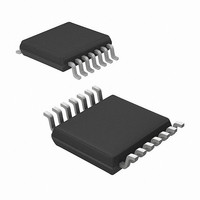
MRF49XA-I/ST Microchip Technology, MRF49XA-I/ST Datasheet - Page 80

MRF49XA-I/ST
Manufacturer Part Number
MRF49XA-I/ST
Description
IC RF TXRX 433/868/915 16-TSSOP
Manufacturer
Microchip Technology
Datasheet
1.MRF49XA-IST.pdf
(102 pages)
Specifications of MRF49XA-I/ST
Package / Case
16-TSSOP
Frequency
433MHz, 868MHz, 915MHz
Data Rate - Maximum
256kbps
Modulation Or Protocol
FHSS, FSK
Applications
Home / Industrial Automation, Remote Access, Security Alarms
Power - Output
7dbm
Sensitivity
-110dBm
Voltage - Supply
2.2 V ~ 3.8 V
Current - Receiving
11mA
Current - Transmitting
15mA
Data Interface
PCB, Surface Mount
Antenna Connector
PCB, Surface Mount
Operating Temperature
-40°C ~ 85°C
Number Of Receivers
1
Number Of Transmitters
2
Wireless Frequency
433 MHz to 915 MHz
Output Power
+ 7 dBm
Operating Supply Voltage
2.5 V, 3.3 V
Maximum Operating Temperature
+ 85 C
Mounting Style
SMD/SMT
Minimum Operating Temperature
- 40 C
Modulation
FHSS, FSK
Lead Free Status / RoHS Status
Lead free / RoHS Compliant
Memory Size
-
Lead Free Status / Rohs Status
Lead free / RoHS Compliant
Other names
579-MRF49XA-1/ST
Available stocks
Company
Part Number
Manufacturer
Quantity
Price
Company:
Part Number:
MRF49XA-I/ST
Manufacturer:
IR
Quantity:
450
Part Number:
MRF49XA-I/ST
Manufacturer:
MICROCHIP/微芯
Quantity:
20 000
TABLE 5-1:
Note 1:
TABLE 5-2:
Note 1:
TABLE 5-3:
Note 1:
DS70590B-page 78
MRF49XA
Operating Temperature
Supply Voltage for RF, Analog and Digital
Circuits
Supply Voltage for Digital I/O
DC Voltage on Open-Collector Outputs
(RFP, RFN)
AC Peak Voltage on Open-Collector
Outputs (RFP, RFN)
Sleep
Idle
TX
TX
RX
Low Battery Voltage Detector
Current Consumption
Wake-up Timer Current
Consumption
V
V
I
I
V
V
V
IL
IH
IL
IH
OL
OH
LBTD
Symbol
2:
2:
Chip Mode
At minimum, V
At maximum, V
Typical Values: T
Typical Values: T
Negative current is defined as the current sourced by the pin.
(1,2)
Parameters
Input Low Voltage
Input High Voltage
Input Low Leakage Current
Input High Leakage Current
Digital Low Output Voltage
Digital Low Output
Low Battery Threshold Detect Programmable in 0.1V
RECOMMENDED OPERATING CONDITIONS
CURRENT CONSUMPTION
I/O PIN INPUT SPECIFICATIONS
(1)
Characteristic
DD
DD
A
A
– 1.5V cannot be lower than 1.2V.
+ 1.5V cannot be higher than 5.5V.
= 25°C, V
= 25°C, V
Sleep clock disabled, all blocks disabled
Oscillator and baseband enabled, clock
output disabled
Power output – 0 dBm, 50Ω load, 433 MHz
868 MHz
915 MHz
At maximum output power, 433 MHz
868 MHz
915 MHz
433 MHz
868 MHz
915 MHz
DD
DD
= 3.3V.
= 3.3V.
(2)
V
V
Condition
DD
DD
V
V
l
I
steps
(1)
OL
OH
Preliminary
Min
IL
IH
-40
2.2
2.2
– 1.5
– 1.5
—
—
= 2 mA
= 0V
= V
= -2 mA
Condition
(1)
DD
, V
—
—
DD
= 3.8V
Typ
3.3
—
—
—
—
V
0.7 x V
DD
2.25
Min
—
—
-1
-1
– 0.4
Min
—
—
—
—
—
—
—
—
—
—
—
—
—
DD
V
V
DD
DD
© 2009 Microchip Technology Inc.
Max
+85
Typ
3.8
3.8
—
—
—
—
—
—
—
+ 1.5
+ 1.5
Typ
0.3
0.6
0.5
1.5
15
16
17
22
23
24
11
12
13
0.3 x V
3.75
Max
0.4
—
—
Max
1
1
1.2
1.7
3.5
—
—
—
26
27
28
13
14
15
1
DD
Unit
°C
V
V
V
V
Unit
Unit
mA
mA
mA
mA
mA
mA
mA
mA
mA
mA
μA
μA
μA
μA
μA
V
V
V
V
V


