EM357-RTR Ember, EM357-RTR Datasheet - Page 186
EM357-RTR
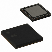
Manufacturer Part Number
EM357-RTR
Description
IC RF TXRX ZIGBEE 192KB 48QFN
Manufacturer
Ember
Specifications of EM357-RTR
Frequency
2.4GHz
Data Rate - Maximum
250kbps
Modulation Or Protocol
802.15.4 Zigbee
Applications
General Purpose
Power - Output
5dBm
Sensitivity
-100dBm
Voltage - Supply
2.1 V ~ 3.6 V
Current - Receiving
26mA
Current - Transmitting
31mA
Data Interface
PCB, Surface Mount
Memory Size
192kB Flash, 12kB RAM
Antenna Connector
PCB, Surface Mount
Operating Temperature
-40°C ~ 85°C
Package / Case
48-QFN
Lead Free Status / RoHS Status
Lead free / RoHS Compliant
Other names
636-1011-2
Available stocks
Company
Part Number
Manufacturer
Quantity
Price
Company:

Part Number:
EM357-RTR
Manufacturer:
SILICON
Quantity:
3 000
Part Number:
EM357-RTR
Manufacturer:
SILICON
Quantity:
20 000


10.4
Calibration
3.
4.
5.
6.
To convert multiple inputs using this approach, repeat steps 4 through 6, loading the desired input
configurations to the ADC_CFG register in step 5. If the inputs can use the same offset/gain correction, just
repeat steps 5 and 6.
Sampling of internal connections GND, VREF/2, and VREF allow for offset and gain calibration of the ADC in
applications where absolute accuracy is important. Offset error is calculated from the minimum input and gain
error is calculated from the full scale input range. Correction using VREF is recommended because VREF is
calibrated by the Ember software against VDD_PADSA. The VDD_PADSA regulator is factory-trimmed to 1.80 V
± 20 mV. If better absolute accuracy is required, the ADC can be configured to use an external reference. The
ADC calibrates as a single-ended measurement. Differential signals require correction of both their inputs.
The following steps outline the calibration procedure
Table 10-5 shows the equations used to calculate the gain and offset correction values.
Equation notes
Calibration
Gain
Offset ( after applying gain correction )
Calibrate VREF against VDD_PADSA.
Determine the ADC gain by sampling independently VREF and GND. Gain is calculated from the slope of
these two measurements.
Apply gain correction.
Determine the ADC offset by sampling GND.
Apply offset correction.
The ADC output is two’s complement. All N are therefore 16-bit two’s complement numbers.
Offset is a 16-bit two’s complement number.
Gain is a 16-bit number representing a gain of 0 to 65535/32768 in 1/32768 steps. The default value is
32768, corresponding to a gain of 1.
N
two’s complement value 32768 as the conversion result. Instead, VGND yields a value close to 57344 when
Set up the DMA to output conversion results to the variable, analogData.
Reset the DMA: Set the ADC_DMARST bit in ADC_DMACFG register.
Define a one sample buffer: Write analogData’s address to the ADC_DMABEG register and set the
ADC_DMASIZE register to 1.
Write the desired offset and gain correction values to the ADC_OFFSET and ADC_GAIN registers.
Start the ADC and the DMA.
Write the desired conversion configuration, with the ADC_EN bit set, to the ADC_CFG register.
Clear the ADC buffer full flag: Write the INT_ADCULDFULL bit to the INT_ADCFLAG register.
Start the DMA in auto wrap mode: Set the ADC_DMAAUTOWRAP and ADC_DMALOAD bits in the
ADC_DMACFG register.
Wait until the INT_ADCULDFULL bit is set in the INT_ADCFLAG register, then read the result from
analogData.
GND
is a sampling of ground. Due to the ADC's internal design, VGND does not yield the minimum 16 bit
Table 10-5. ADC Gain and offset correction equations
Final
10-7
Correction value
32768
2
×
(
57344
×
(
N
VREF
−
16384
N
GND
−
N
)
GND
)
EM351 / EM357
120-035X-000G
Related parts for EM357-RTR
Image
Part Number
Description
Manufacturer
Datasheet
Request
R

Part Number:
Description:
MODULE EM357 PA/LNA W/ANT TG
Manufacturer:
Ember
Datasheet:

Part Number:
Description:
MODULE EM357 NO PA/LNA W/ANT TG
Manufacturer:
Ember
Datasheet:

Part Number:
Description:
MODULE EM357 NO PA/LNA W/RF CONN
Manufacturer:
Ember
Datasheet:
Part Number:
Description:
MODULE EM357 PA/LNA W/RF CONN
Manufacturer:
Ember
Datasheet:

Part Number:
Description:
IC RF TXRX ZIGBEE 192KB 48QFN
Manufacturer:
Ember
Datasheet:

Part Number:
Description:
KIT DEV EMBER ZIGBEE W/PCWH
Manufacturer:
Custom Computer Services Inc (CCS)

Part Number:
Description:
PROGRAMMER USB FLASH EM250/260
Manufacturer:
Ember
Datasheet:

Part Number:
Description:
IC ZIGBEE SYSTEM-ON-CHIP 40-QFN
Manufacturer:
Ember
Datasheet:
Part Number:
Description:
IC ZIGBEE SYSTEM-ON-CHIP 48-QFN
Manufacturer:
Ember
Datasheet:
Part Number:
Description:
IC RF TXRX ZIGBEE 128KB 48QFN
Manufacturer:
Ember
Datasheet:

Part Number:
Description:
INSIGHT ADAPTER FOR EM2XX
Manufacturer:
Ember
Datasheet:
Part Number:
Description:
PROGRAMMER USB FLASH EM250/260
Manufacturer:
Ember
Datasheet:
Part Number:
Description:
IC ZIGBEE SYSTEM-ON-CHIP 40-QFN
Manufacturer:
Ember
Datasheet:
Part Number:
Description:
IC ZIGBEE SYSTEM-ON-CHIP 48-QFN
Manufacturer:
Ember
Datasheet:
Part Number:
Description:
IC RF TXRX ZIGBEE 128KB 48QFN
Manufacturer:
Ember
Datasheet: