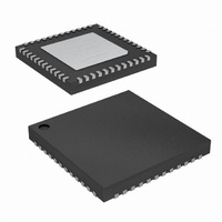
CYWUSB6934-48LTXC Cypress Semiconductor Corp, CYWUSB6934-48LTXC Datasheet - Page 22

CYWUSB6934-48LTXC
Manufacturer Part Number
CYWUSB6934-48LTXC
Description
IC WIRELESS USB 2.4GHZ 48VQFN
Manufacturer
Cypress Semiconductor Corp
Series
WirelessUSB™r
Datasheet
1.CYWUSB6934-48LTXC.pdf
(33 pages)
Specifications of CYWUSB6934-48LTXC
Package / Case
48-VQFN Exposed Pad, 48-HVQFN, 48-SQFN, 48-DHVQFN
Frequency
2.4GHz
Data Rate - Maximum
62.5kbps
Modulation Or Protocol
GFSK
Applications
General Purpose
Power - Output
0dBm
Sensitivity
-90dBm
Voltage - Supply
2.7 V ~ 3.6 V
Current - Receiving
57.7mA
Current - Transmitting
69.1mA
Data Interface
PCB, Surface Mount
Antenna Connector
PCB, Surface Mount
Operating Temperature
0°C ~ 70°C
Wireless Frequency
2.4 GHz
Operating Supply Voltage
2.7 V to 3.6 V
Maximum Operating Temperature
+ 70 C
Mounting Style
SMD/SMT
Minimum Operating Temperature
0 C
Lead Free Status / RoHS Status
Lead free / RoHS Compliant
Memory Size
-
Lead Free Status / Rohs Status
Lead free / RoHS Compliant
Other names
428-2984
Available stocks
Company
Part Number
Manufacturer
Quantity
Price
Part Number:
CYWUSB6934-48LTXC
Manufacturer:
CYPRESS/赛普拉斯
Quantity:
20 000
Pin Definitions
Table 35. Pin Description Table for the CYWUSB6932/CYWUSB6934
Document 38-16007 Rev. *J
6, 9, 16, 28,
1, 2, 3, 4, 7,
29, 32, 41,
12, 15, 17,
18, 27, 30,
31, 36, 37,
39, 40, 43,
42, 44, 45
8, 10, 11,
Pin QFN
Exposed
Paddle
47, 48
46
38
35
26
33
14
34
20
19
21
23
24
25
22
13
5
RFIN
RFOUT
X13
X13IN
X13OUT
PD
RESET
PACTL
DIO
DIOVAL
IRQ
MOSI
MISO
SCK
SS
VCC
GND
NC
GND
Name
Output /Hi-Z
Output/Hi-Z
Output/Hi-Z
Output
Type
Input
Input
Input
Input
Input
Input
Input
Input
GND
GND
VCC
N/A
I/O
I/O
I/O
Default
Output System Clock . Buffered 13-MHz system clock.
Output IRQ . Interrupt and SERDES Bypass Mode DIOCLK.
Input
Input
Input
Input
Hi-Z
N/A
N/A
N/A
N/A
N/A
N/A
N/A
N/A
N/A
H
L
L
RF Input . Modulated RF signal received (CYWUSB6934 only).
RF Output . Modulated RF signal to be transmitted.
Crystal Input . (refer to Section ).
Crystal Input . (refer to Section ).
Power Down . Asserting this input (low), will put the
CYWUSB6932/CYWUSB6934 in the Suspend Mode (X13OUT is 0 when PD is
low).
Active LOW Reset . Device reset.
PACTL . External Power Amplifier control. Pull-down or make output.
Data Input/Output. SERDES Bypass Mode Data Transmit/Receive.
Data I/O Valid . SERDES Bypass Mode Data Transmit/Receive Valid.
Master-Output-Slave-Input Data . SPI data input pin.
Master-Input-Slave-Output Data . SPI data output pin.
SPI Input Clock . SPI clock.
Slave Select Enable . SPI enable.
V
Ground = 0V .
Must be tied to Ground.
Must be tied to Ground.
CC
= 2.7V to 3.6V.
Description
CYWUSB6934
CYWUSB6932
Page 22 of 33
[+] Feedback


