MC13202FC Freescale Semiconductor, MC13202FC Datasheet
MC13202FC
Specifications of MC13202FC


Related parts for MC13202FC

MC13202FC Summary of contents
Page 1
... ZigBee networking. For Freescale reserves the right to change the detail specifications as may be required to permit improvements in the design of its products. © Freescale Semiconductor, Inc., 2005, 2006, 2007, 2008. All rights reserved. Device MC13202FC MC13202FCR2 (Tape and Reel) Contents 1 Introduction . . . . . . . . . . . . . . . . . . . . . . . . . . 1 2 Features . . . . . . . . . . . . . . . . . . . . . . . . . . . . . 2 3 Block Diagrams . . . . . . . . . . . . . . . . . . . . . . . 4 4 Data Transfer Modes ...
Page 2
... Operates on one of 16 selectable channels in the 2.4 GHz band • dBm nominal output power, programmable from -27 dBm to +3 dBm typical • Receive sensitivity of <-92 dBm (typical PER, 20-byte packet, much better than the 802.15.4 Standard of -85 dBm 2 MC13202 Technical Data, Rev. 1.5 Freescale Semiconductor ...
Page 3
... User networks built on the 802.15.4 MAC standard. 3. ZigBee-compliant network stack. 2.1.1 Simple MAC (SMAC) • Small memory footprint (about 3 Kbytes typical) • Supports point-to-point and star network configurations • Proprietary networks • Source code and application examples provided Freescale Semiconductor MC13202 Technical Data, Rev. 1.5 3 ...
Page 4
... Logic Packet Digital Processor Regulator H Cry stal Regulator VCO Receiv e RAM Regulator Arbiter Sequence Manager (Control Logic) IRQ Sy mbol Arbiter Arbiter Generation Freescale Semiconductor VDDA VBATT VDDINT VDDD VDDVCO RXTXEN CE MOSI MISO SPICLK ATTN RST GPIO1 GPIO2 GPIO3 GPIO4 GPIO5 GPIO6 ...
Page 5
... MC13202 adds a four-byte preamble, a one-byte Start of Frame Delimiter (SFD), and a one-byte Frame Length Indicator (FLI) before the data. A Frame Check Sequence (FCS) is calculated and appended to the end of the data. 4 bytes 1 byte Preamble SFD Freescale Semiconductor Control SPI Logic and GPIO Buffer RAM Figure 2. System Level Block Diagram ...
Page 6
... Figure 4. Reported Power Level versus Input Power in CCA Mode 6 NOTE 802.15.4 Ac curac y and range Requirements -90 -80 -70 -60 Input Pow er (dBm) MC13202 Technical Data, Rev. 1.5 Figure 5 shows energy -50 Freescale Semiconductor ...
Page 7
... In streaming mode, the data is fed to the MC13202 on a word-by-word basis with an interrupt serving as a notification that the MC13202 is ready for more data. This continues until the whole packet is transmitted. Freescale Semiconductor 802.15.4 Accuracy and Range Requirements -75 ...
Page 8
... Value V -0.3 to 3.6 DDINT Vin -0 0.3) DDINT P 10 max T 125 J T -55 to 125 stg Min Typ Max 2.0 2.7 3.4 2.405 - 2.480 - 30% V DDINT 70 DDINT V DDINT - - 8 MHz Only Freescale Semiconductor Unit Vdc dBm °C °C Unit Vdc GHz ° MHz dBm ...
Page 9
... Output Low Voltage ( mA) (All digital outputs attain specified low power current, all GPIO and other digital IO must be handled properly. See Power Considerations”. 2 CLKO frequency at default value of 32.786 kHz. Freescale Semiconductor Table 3. DC Electrical Characteristics , °C, unless otherwise noted) DDINT A Symbol ) ...
Page 10
... MHz, unless otherwise noted.) A ref Symbol P out EVM MC13202 Technical Data, Rev. 1.5 Symbol Min Typ Max SENS - -92 - per - -92 - max - 200 - - 80 Min Typ Max - - 250 - - - -70 - Freescale Semiconductor Unit dBm dBm dBm kHz ppm Unit dBm dBm dBm % dB kbps dBc dBc ...
Page 11
... CT_Bias MC1320x Characteristic RFIN Pins for internal T/R switch configuration, TX mode RFIN Pins for internal or external T/R switch configuration, RX mode PAO Pins for external T/R switch configuration, TX mode Freescale Semiconductor Table 6. Digital Timing Specifications SPI timing parameters are referenced to Min 125 50 ...
Page 12
... Master In/Slave Out (MISO) - The MC13202 presents data to the master on the MISO output Current drain in the various modes is listed in Definition NOTE MC13202 Technical Data, Rev. 1.5 Table 3, DC Electrical Transition Time To or From Idle Idle Idle (300 + 1/CLKO) µs to Idle 144 µs from Idle 144 µs from Idle Freescale Semiconductor ...
Page 13
... MISO line. Although an MC13202 transaction is three or more SPI bursts long, the timing of a single SPI burst is shown SPIC alid M ISO alid SPI digital timing specifications are shown in Freescale Semiconductor Figure RxD MISO TxD MOSI Sclk SPICLK Chip Enable (CE) Figure 7. SPI Interface Figure 8. SPI Burst ...
Page 14
... After the final SPI burst negated to high to signal the end of the transaction. Refer to the MC13202 Reference Manual, (MC13202RM) for more details on SPI registers and transaction types. An example SPI read transaction with a 2-byte payload is shown rst lid V a lid Figure 9. SPI Read Transaction Diagram MC13202 Technical Data, Rev. 1.5 Figure lid Freescale Semiconductor ...
Page 15
... GPIO2 Digital Input/ Output General Purpose Input/Output GPIO1 Digital Input/ Output General Purpose Input/Output 1. 12 RST Digital Input Freescale Semiconductor Table 8. Pin Function Description Description RF input/output negative. RF input/output positive. Bias voltage/control signal for external RF components Tie to Ground. Test mode pin. When gpio_alt_en, Register 9, Bit GPIO2 functions as a “ ...
Page 16
... Open drain device. Ω Programmable 40 k internal pull-up. Interrupt can be serviced every 6 µs with <20 pF load. Optional external pull-up must be >4 k Decouple to ground. 2.0 to 3.4 V. Decouple to ground. See Footnote 1 See Footnote 1 See Footnote 1 Connect to 16 MHz crystal and load capacitor. Freescale Semiconductor Ω . ...
Page 17
... During low power modes, input must remain driven by MCU default MISO is tri-stated when CE is negated. For low power operation, miso_hiz_en (Bit 11, Register 07) should be set to zero so that MISO is driven low when CE is negated. Freescale Semiconductor Description Crystal Reference oscillator output Note: Do not load this pin by using MHz source ...
Page 18
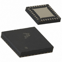
... RFIN_M 2 RFIN_P 3 CT_Bias PAO_P 6 PAO_M GPIO4 MC13202 Figure 10. Pin Connections (Top View) MC13202 Technical Data, Rev. 1 GPIO6 23 GPIO5 22 VDDINT 21 VDDD 20 IRQ MISO 17 MOSI 16 Freescale Semiconductor ...
Page 19
... A different board layout may require a different external load capacitor value. The on-chip trim capability may be used to determine the closest standard value by adjusting the trim value via the SPI and observing the frequency at CLKO. Each internal trim load capacitor has a trim range of approximately steps. Freescale Semiconductor MC13202 Technical Data, Rev. 1.5 19 ...
Page 20
... Table 9. MC13202 Crystal Specifications Value Unit 16.000000 MHz 2 ± 10 ppm 3 ± 15 ppm ± 2 ppm 5 Ω <2 pF MC13202 Technical Data, Rev. 1.5 C10 6.8pF C11 6.8pF Table 9. A number of the stated 1 Condition at 25 °C Over desired temperature range max max max fundamental Freescale Semiconductor ...
Page 21
... Use only STOP2 and STOP3 modes (not STOP1) with these devices where the GPIO states are retained. The MCU must retain control of the MC13202 IO during low power operation. — As stated above all unused GPIO should be programmed as outputs low for lowest power and no floating inputs. Freescale Semiconductor NOTE MC13202 Technical Data, Rev. 1.5 21 ...
Page 22
... RF interface pins and the associated analog blocks. Notice that separate PA blocks are associated with RFIN_x and PAO_x signal pairs. The RF interface allows both single port differential operation and dual port differential operation Figure 12. RF Interface Pins MC13202 Technical Data, Rev. 1 Freescale Semiconductor ...
Page 23
... In dual port operation, the RFIN_P and RFIN_N are inputs only, the internal RX switch to the LNA is enabled to receive, and the associated TX PA stays disabled. Pins PAO_P and PAO_N become the differential output pins and the associated enabled for transmit. Freescale Semiconductor MC13202/03 RFIN_P (PAO_P) ...
Page 24
... B a lun Using External Antenna Switch with LNA Figure 14. Dual Port RF Configuration Examples ass M C 1320 2/ ias ( tl ass RX Antenna L1 TX Antenna Bypass MC13202 Technical Data, Rev. 1 RFIN_P (PAO_P) RFIN_M (PAO_M) MC13202/03 VDDA Bypass L4 L5 CT_Bias PAO_P PAO_M Using Dual Antenna Freescale Semiconductor ...
Page 25
... The ct_bias_inv bit causes the sense of the active state to change or invert based on Bit 13’s setting. In this manner, the user can select the CT_Bias as a control signal for external components and make the control signal active high or active low. Freescale Semiconductor shows the model for Register 07 with the RF interface control bits Register 07 ...
Page 26
... Dual Port Mode selected where RFIN_M and RFIN_P are inputs only and PAO_P and PAO_N are separate outputs. (This is default operation). RF_switch_mode CT_Bias_inv MC13202 Technical Data, Rev. 1.5 Operation Table 11. Table 11. This bit only Section 9.1.1, “Single Section 9.1.2, “Dual Port CT_Bias Hi Freescale Semiconductor ...
Page 27
... Capacitor C2 provides some high frequency bypass to the DC bias point. The L3/C1 network provides a simple bandpass filter to limit out-of-band harmonics from the transmitter PAO_M 5 1.8nH PAO_P 2 RFIN_P 1 RFIN_M 3 CT_Bias L4 MC1320x 1.8nH Figure 16. RF Single Port Application with an F-Antenna Freescale Semiconductor RF_switch_mode CT_Bias_inv ...
Page 28
... LEADS, AND DIE ATTACH PAD. 6. FOR ANVIL SINGULATED QFN PACKAGES, MAXIMUM DRAFT ANGLE IS 12°. 0.217 0.137 0.217 0.137 (0.25) (0.1) DETAIL S PREFERRED BACKSIDE PIN 1 INDEX DETAIL S DETAIL M PREFERRED BACKSIDE PIN 1 INDEX (90 ) 0.39 2X 0.31 0.1 2X 0.0 DETAIL T BACKSIDE PIN 1 INDEX OPTION Freescale Semiconductor ...
Page 29
... Freescale Semiconductor NOTES MC13202 Technical Data, Rev. 1.5 ...
Page 30
... Freescale Semiconductor products are not designed, intended, or authorized for use as components in systems intended for surgical implant into the body, or other applications intended to support or sustain life, or for any other application in which the failure of the Freescale Semiconductor product could create a situation where personal injury or death may occur. Should Buyer purchase ...