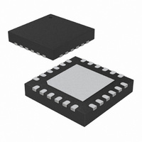
ATA5773-PXQW Atmel, ATA5773-PXQW Datasheet - Page 175

ATA5773-PXQW
Manufacturer Part Number
ATA5773-PXQW
Description
XMITTR UHF ASK/FSK 310MHZ 24VQFN
Manufacturer
Atmel
Datasheet
1.ATA5773-DK1.pdf
(219 pages)
Specifications of ATA5773-PXQW
Frequency
310MHz ~ 350MHz
Modulation Or Protocol
UHF
Power - Output
8dBm
Voltage - Supply
2 V ~ 4 V
Current - Transmitting
9.8mA
Data Interface
PCB, Surface Mount
Memory Size
4kB Flash, 256B EEPROM, 256B SRAM
Antenna Connector
PCB, Surface Mount
Operating Temperature
-40°C ~ 85°C
Package / Case
24-VQFN Exposed Pad, 24-HVQFN, 24-SQFN, 24-DHVQFN
Processor Series
ATA5x
Core
AVR8
Data Bus Width
8 bit
Program Memory Type
Flash
Program Memory Size
4 KB
Data Ram Size
256 B
Interface Type
SPI, USI
Maximum Clock Frequency
4 MHz
Number Of Programmable I/os
12
Number Of Timers
2
Maximum Operating Temperature
+ 85 C
Mounting Style
SMD/SMT
Minimum Operating Temperature
- 40 C
On-chip Adc
10 bit, 12 Channel
Lead Free Status / RoHS Status
Lead free / RoHS Compliant
Applications
-
Sensitivity
-
Data Rate - Maximum
-
Current - Receiving
-
Lead Free Status / Rohs Status
Details
Available stocks
Company
Part Number
Manufacturer
Quantity
Price
Company:
Part Number:
ATA5773-PXQW
Manufacturer:
ATMEL
Quantity:
3 500
Part Number:
ATA5773-PXQW
Manufacturer:
ATMEL/爱特梅尔
Quantity:
20 000
- Current page: 175 of 219
- Download datasheet (4Mb)
4.23.8
4.23.8.1
4.23.8.2
4.23.8.3
9137E–RKE–12/10
High-voltage Serial Programming Algorithm
Enter High-voltage Serial Programming Mode
Considerations for Efficient Programming
Chip Erase
To program and verify the Atmel
the following sequence is recommended (See instruction formats in
The following algorithm puts the device in High-voltage Serial Programming mode:
1. Apply 4.5 - 5.5V between V
2. Set RESET pin to “0” and toggle SCI at least six times.
3. Set the Prog_enable pins listed in
4. Apply V
5. Shortly after latching the Prog_enable signature, the device will activly output data on
6. Wait at least 50 µs before giving any serial instructions on SDI/SII.
Table 4-69.
The loaded command and address are retained in the device during programming. For effi-
cient programming, the following should be considered.
• The command needs only be loaded once when writing or reading multiple memory
• Skip writing the data value 0xFF that is the contents of the entire EEPROM (unless the
• Address High byte needs only be loaded before programming or reading a new 256 word
The Chip Erase will erase the Flash and EEPROM
are not reset until the Program memory has been completely erased. The Fuse bits are not
changed. A Chip Erase must be performed before the Flash and/or EEPROM are
re-programmed.
Note:
1. Load command “Chip Erase” (see
2. Wait after Instr. 3 until SDO goes high for the “Chip Erase” cycle to finish.
3. Load Command “No Operation”.
Supply Voltage
V
4.5V
5.5V
locations.
EESAVE Fuse is programmed) and Flash after a Chip Erase.
window in Flash or 256 byte EEPROM. This consideration also applies to Signature bytes
reading.
CC
100 ns.
t
has been latched.
the Prog_enable[2]/SDO pin, and the resulting drive contention may increase the
power consumption. To minimize this drive contention, release the Prog_enable[2] pin
after t
HVRST
1. The EEPROM memory is preserved during Chip Erase if the EESAVE Fuse is programmed.
HVRST
after the High-voltage has been applied to ensure the Prog_enable signature
HVRST
High-voltage Reset Characteristics
has elapsed.
- 5.5V to RESET. Keep the Prog_enable pins unchanged for at least
RESET Pin High-voltage Threshold
CC
®
and GND.
ATtiny44V in the High-voltage Serial Programming mode,
V
11.5V
11.5V
HVRST
Table 4-68 on page 174
Table 4-70 on page
(1)
Atmel ATA5771/73/74
memories plus Lock bits. The Lock bits
178).
Minimum High-voltage Period for
to “000” and wait at least
Latching Prog_enable
Table 4-70 on page
100 ns
100 ns
t
HVRST
178):
175
Related parts for ATA5773-PXQW
Image
Part Number
Description
Manufacturer
Datasheet
Request
R

Part Number:
Description:
BOARD XMITTER FOR ATA5773 315MHZ
Manufacturer:
Atmel
Datasheet:

Part Number:
Description:
Microcontroller With Uhf Ask/fsk Transmitter
Manufacturer:
ATMEL Corporation
Datasheet:

Part Number:
Description:
DEV KIT FOR AVR/AVR32
Manufacturer:
Atmel
Datasheet:

Part Number:
Description:
INTERVAL AND WIPE/WASH WIPER CONTROL IC WITH DELAY
Manufacturer:
ATMEL Corporation
Datasheet:

Part Number:
Description:
Low-Voltage Voice-Switched IC for Hands-Free Operation
Manufacturer:
ATMEL Corporation
Datasheet:

Part Number:
Description:
MONOLITHIC INTEGRATED FEATUREPHONE CIRCUIT
Manufacturer:
ATMEL Corporation
Datasheet:

Part Number:
Description:
AM-FM Receiver IC U4255BM-M
Manufacturer:
ATMEL Corporation
Datasheet:

Part Number:
Description:
Monolithic Integrated Feature Phone Circuit
Manufacturer:
ATMEL Corporation
Datasheet:

Part Number:
Description:
Multistandard Video-IF and Quasi Parallel Sound Processing
Manufacturer:
ATMEL Corporation
Datasheet:

Part Number:
Description:
High-performance EE PLD
Manufacturer:
ATMEL Corporation
Datasheet:

Part Number:
Description:
8-bit Flash Microcontroller
Manufacturer:
ATMEL Corporation
Datasheet:

Part Number:
Description:
2-Wire Serial EEPROM
Manufacturer:
ATMEL Corporation
Datasheet:


