ATA5773-PXQW Atmel, ATA5773-PXQW Datasheet - Page 7

ATA5773-PXQW
Manufacturer Part Number
ATA5773-PXQW
Description
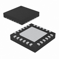
XMITTR UHF ASK/FSK 310MHZ 24VQFN
Manufacturer
Atmel
Datasheet
1.ATA5773-DK1.pdf
(219 pages)
Specifications of ATA5773-PXQW
Frequency
310MHz ~ 350MHz
Modulation Or Protocol
UHF
Power - Output
8dBm
Voltage - Supply
2 V ~ 4 V
Current - Transmitting
9.8mA
Data Interface
PCB, Surface Mount
Memory Size
4kB Flash, 256B EEPROM, 256B SRAM
Antenna Connector
PCB, Surface Mount
Operating Temperature
-40°C ~ 85°C
Package / Case
24-VQFN Exposed Pad, 24-HVQFN, 24-SQFN, 24-DHVQFN
Processor Series
ATA5x
Core
AVR8
Data Bus Width
8 bit
Program Memory Type
Flash
Program Memory Size
4 KB
Data Ram Size
256 B
Interface Type
SPI, USI
Maximum Clock Frequency
4 MHz
Number Of Programmable I/os
12
Number Of Timers
2
Maximum Operating Temperature
+ 85 C
Mounting Style
SMD/SMT
Minimum Operating Temperature
- 40 C
On-chip Adc
10 bit, 12 Channel
Lead Free Status / RoHS Status
Lead free / RoHS Compliant
Applications
-
Sensitivity
-
Data Rate - Maximum
-
Current - Receiving
-
Lead Free Status / Rohs Status
Details
Available stocks
Company
Part Number
Manufacturer
Quantity
Price
Company:
Part Number:
ATA5773-PXQW
Manufacturer:
ATMEL
Quantity:
3 500
Part Number:
ATA5773-PXQW
Manufacturer:
ATMEL/爱特梅尔
Quantity:
20 000
3. Functional Description
9137E–RKE–12/10
Figure 1-1 on page 2
controller and the RF part for a typical application. In the recommended application circuits the
clock output of the RF transmitter is connected to the microcontroller in order to be able to
generate data rate with tolerance lower than 3%. The transmitter’s crystal oscillator (XTO),
Phase Locked Loop (PLL) and clock generation are started using pin ENABLE. The Power
amplifier (PA) is activated using the connection to the pin PA_ENABLE. The FSK modulation
is performed due to pulling of the crystal load capacitance for this purpose the microcontroller
out put port together with an external switch applies this modulation technique. For the ASK
modulation the power amplifier will be switched on and of by modulating the PA_ENABLE pin
due to the data.
To wake up the system from standby mode at least one event is required, which will be
performed by pushing tone button. After this event the microcontroller starts up with the inter-
nal RC oscillator. For the TX operation the user software must additionally control just 2 pins,
the pin ENABLE and pin PA_ENABLE. In case of the FSK modulation one additional connec-
tion from microcontroller is necessary to perform the pulling of the crystal load capacitance.
If ENABLE and PA_ENABLE are set to LOW the transmitter is in standby mode with the suit-
able mode setting of the microcontroller (MCU) the power consumption will be reduced.
If ENABLE is set to HIGH and PA_ENABLE to LOW, the XTO, PLL, and the Clock driver of the
RF transmitter are activated and the VCO frequency is 32 times the XTO frequency. The
Atmel ATA5771 and Atmel ATA5774 require typically shorter than 1 ms until the PLL is locked
and the transmitter’s clock output is stable, while the Atmel ATA5773 requires time shorter
than 3 ms for this progress.
If both ENABLE and PA_ENABLE are set to HIGH the whole RF transmitter (XTO, PLL, Clock
driver and power Amplifier) is activated. The ASK modulation is achieved by switching on and
off the power amplifier via pin PA_ENABLE. The FSK modulation is performed by pulling the
crystal load capacitor which will change the reference frequency of the PLL due to the data.
The microcontroller modulates the load capacitance of the crystal using an external switch. A
MOS transistor with a low parasitic capacitance is recommended to be used for this purpose.
During the FSK modulation is the PA_ENABLE pin set to HIGH.
To generate the data for the telegram the internal RC oscillator of the microcontroller is not
accurate enough because this will be affected by ambient temperature and operating voltage.
To reduce the variation of the data rate lower than 3% the clock frequency generated by the
RF transmitter should be used as a reference. The MCU has to wait at least longer than 3 ms
for ATA5773 after setting ENABLE to HIGH, before the clock output from the RF transmitter
can be used. For ATA5771 and ATA5774 the MCU must wait longer than 1 ms until the clock
output is stable. The clock output with the crystal tolerance is connected to the timer0 of the
MCU. This timer clocks the USI to generate the data rate. In the Two serial synchronous data
transfer modes will be provided by USI. This will be pass out with different physical I/O ports,
two wire mode is used for ASK and the three wire mode for FSK.
and
Figure 1-2 on page 3
show the interconnections between the micro-
Atmel ATA5771/73/74
7


