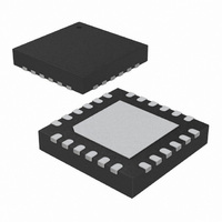
ATA5771-PXQW Atmel, ATA5771-PXQW Datasheet - Page 125

ATA5771-PXQW
Manufacturer Part Number
ATA5771-PXQW
Description
XMITTR UHF ASK/FSK 868MHZ 24VQFN
Manufacturer
Atmel
Datasheet
1.ATA5773-DK1.pdf
(219 pages)
Specifications of ATA5771-PXQW
Frequency
868MHz ~ 928MHz
Modulation Or Protocol
UHF
Power - Output
8dBm
Voltage - Supply
2 V ~ 4 V
Current - Transmitting
9.8mA
Data Interface
PCB, Surface Mount
Memory Size
4kB Flash, 256B EEPROM, 256B SRAM
Antenna Connector
PCB, Surface Mount
Operating Temperature
-40°C ~ 85°C
Package / Case
24-VQFN Exposed Pad, 24-HVQFN, 24-SQFN, 24-DHVQFN
Processor Series
ATA5x
Core
AVR8
Data Bus Width
8 bit
Program Memory Type
Flash
Program Memory Size
4 KB
Data Ram Size
256 B
Interface Type
SPI, USI
Maximum Clock Frequency
4 MHz
Number Of Programmable I/os
12
Number Of Timers
2
Maximum Operating Temperature
+ 85 C
Mounting Style
SMD/SMT
Minimum Operating Temperature
- 40 C
On-chip Adc
10 bit, 12 Channel
Lead Free Status / RoHS Status
Lead free / RoHS Compliant
Applications
-
Sensitivity
-
Data Rate - Maximum
-
Current - Receiving
-
Lead Free Status / Rohs Status
Details
Available stocks
Company
Part Number
Manufacturer
Quantity
Price
Company:
Part Number:
ATA5771-PXQW
Manufacturer:
ATMEL
Quantity:
218
- Current page: 125 of 219
- Download datasheet (4Mb)
4.18
4.18.1
4.18.2
9137E–RKE–12/10
USI – Universal Serial Interface
Features
Overview
•
•
•
•
•
•
The Universal Serial Interface (USI), provides the basic hardware resources needed for serial
communication. Combined with a minimum of control software, the USI allows significantly
higher transfer rates and uses less code space than solutions based on software only. Inter-
rupts are included to minimize the processor load.
A simplified block diagram of the USI is shown in
pins. CPU accessible I/O Registers, including I/O bits and I/O pins, are shown in bold. The
device-specific I/O Register and bit locations are listed in the
tion” on page
Figure 4-52. Universal Serial Interface, Block Diagram
The 8-bit Shift Register is directly accessible via the data bus and contains the incoming and
outgoing data. The register has no buffering so the data must be read as quickly as possible to
ensure that no data is lost. The most significant bit is connected to one of two output pins
depending of the wire mode configuration. A transparent latch is inserted between the Serial
Register Output and output pin, which delays the change of data output to the opposite clock
edge of the data input sampling. The serial input is always sampled from the Data Input (DI)
pin independent of the configuration.
Two-wire Synchronous Data Transfer (Master or Slave)
Three-wire Synchronous Data Transfer (Master or Slave)
Data Received Interrupt
Wakeup from Idle Mode
In Two-wire Mode: Wake-up from All Sleep Modes, Including Power-down Mode
Two-wire Start Condition Detector with Interrupt Capability
39.
USIDR
USISR
USICR
2
4-bit Counter
3
2
1
0
3
2
1
0
D Q
LE
[1]
TIM0 COMP
Figure
0
1
Atmel ATA5771/73/74
4-52. For the actual placement of I/O
Two-wire Clock
Control Unit
Section 4.9.10 “Register Descrip-
CLOCK
HOLD
DO
DI/SDA
USCK/SCL
(Output only)
(Input/Open Drain)
(Input/Open Drain)
125
Related parts for ATA5771-PXQW
Image
Part Number
Description
Manufacturer
Datasheet
Request
R

Part Number:
Description:
BOARD XMITTER FOR ATA5771 868MHZ
Manufacturer:
Atmel
Datasheet:

Part Number:
Description:
Manufacturer:
ATMEL Corporation
Datasheet:

Part Number:
Description:
DEV KIT FOR AVR/AVR32
Manufacturer:
Atmel
Datasheet:

Part Number:
Description:
INTERVAL AND WIPE/WASH WIPER CONTROL IC WITH DELAY
Manufacturer:
ATMEL Corporation
Datasheet:

Part Number:
Description:
Low-Voltage Voice-Switched IC for Hands-Free Operation
Manufacturer:
ATMEL Corporation
Datasheet:

Part Number:
Description:
MONOLITHIC INTEGRATED FEATUREPHONE CIRCUIT
Manufacturer:
ATMEL Corporation
Datasheet:

Part Number:
Description:
AM-FM Receiver IC U4255BM-M
Manufacturer:
ATMEL Corporation
Datasheet:

Part Number:
Description:
Monolithic Integrated Feature Phone Circuit
Manufacturer:
ATMEL Corporation
Datasheet:

Part Number:
Description:
Multistandard Video-IF and Quasi Parallel Sound Processing
Manufacturer:
ATMEL Corporation
Datasheet:

Part Number:
Description:
High-performance EE PLD
Manufacturer:
ATMEL Corporation
Datasheet:

Part Number:
Description:
8-bit Flash Microcontroller
Manufacturer:
ATMEL Corporation
Datasheet:

Part Number:
Description:
2-Wire Serial EEPROM
Manufacturer:
ATMEL Corporation
Datasheet:


