CYWUSB6934-28SEC Cypress Semiconductor Corp, CYWUSB6934-28SEC Datasheet - Page 16
CYWUSB6934-28SEC
Manufacturer Part Number
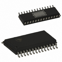
CYWUSB6934-28SEC
Description
IC WIRELESS USB 2.4GHZ 28-SOIC
Manufacturer
Cypress Semiconductor Corp
Specifications of CYWUSB6934-28SEC
Frequency
2.4GHz
Data Rate - Maximum
62.5kbps
Modulation Or Protocol
DSSS, GFSK
Applications
HID, PC, Peripheral Gaming Devices
Power - Output
0dBm
Sensitivity
-90dBm
Voltage - Supply
2.7 V ~ 3.6 V
Data Interface
PCB, Surface Mount
Antenna Connector
PCB, Surface Mount
Operating Temperature
0°C ~ 70°C
Package / Case
28-SOIC
Operating Temperature (min)
0C
Operating Temperature (max)
70C
Operating Temperature Classification
Commercial
Operating Supply Voltage (min)
2.7V
Operating Supply Voltage (typ)
3V
Operating Supply Voltage (max)
3.6V
Lead Free Status / RoHS Status
Contains lead / RoHS non-compliant
Memory Size
-
Current - Transmitting
-
Current - Receiving
-
Lead Free Status / Rohs Status
Not Compliant
Other names
428-1580-5
Available stocks
Company
Part Number
Manufacturer
Quantity
Price
Company:

Part Number:
CYWUSB6934-28SEC
Manufacturer:
CY
Quantity:
22 751


Table 16. Transmit SERDES Data
Table 17. Transmit SERDES Valid
Table 18. PN Code
Note
Document 38-16007 Rev. *J
7:0 Data
7:0
63:0
63 62 61 60 59 58 57 56 55 54 53 52 51 50 49 48 47 46 45 44 43 42 41 40 39 38 37 36 35 34 33 32
31 30 29 28 27 26 25 24 23 22 21 20 19 18 17 16 15 14 13 12 11 10 9
6. The Valid bit in the Transmit SERDES Valid register (Reg 0x10) is used to mark whether the radio will send data or preamble during that bit time of the data byte. Data
Bit Name
Bit
Bit
is sent LSB first. The SERDES will continue to send data until there are no more VALID bits in the shifter. For example, writing 0x0F to the Transmit SERDES Valid
register (Reg 0x10) will send half a byte.
Valid
Name
7
7
PN Codes
Address 0x18
Address 0x14
Addr: 0x0F
Addr: 0x10
Name
Addr: 0x11-18
[6]
by bit 4, followed by bit 5, followed by bit 6, followed by bit 7.
Transmit Data. The over-the-air transmitted order is bit 0 followed by bit 1, followed by bit 2, followed by bit 3, followed
The Valid bits are used to determine which of the bits in the Transmit SERDES Data register (reg 0x0F) are valid.
1 = Valid transmit bit.
0 = Invalid transmit bit.
The value inside the 8 byte PN code register is used as the spreading code for DSSS communication. All 8 bytes
can be used together for 64 chips/bit PN code communication, or the registers can be split into two sets of 32
chips/bit PN codes and these can be used alone or with each other to accomplish faster data rates. Not any 64
chips/bit value can be used as a PN code as there are certain characteristics that are needed to minimize the
possibility of multiple PN codes interfering with each other or the possibility of invalid correlation. The over-the-air
order is bit 0 followed by bit 1... followed by bit 62, followed by bit 63.
6
6
5
5
Address 0x17
Address 0x13
4
4
REG_TX_VALID
REG_TX_DATA
REG_PN_CODE
Valid
Data
Description
Description
Description
3
3
Address 0x16
Address 0x12
2
2
8
7
0x1E8B6A3DE0E9B222
6
1
1
CYWUSB6934
CYWUSB6932
Default: 0x00
Default: 0x00
Address 0x15
5
Address 0x11
Default:
4
3
Page 16 of 33
2
0
0
1
0
[+] Feedback
Related parts for CYWUSB6934-28SEC
Image
Part Number
Description
Manufacturer
Datasheet
Request
R

Part Number:
Description:
IC USB WIRELESS 2.4GHZ 48VQFN
Manufacturer:
Cypress Semiconductor Corp
Datasheet:
Part Number:
Description:
IC WIRELESS USB 2.4GHZ 48VQFN
Manufacturer:
Cypress Semiconductor Corp
Datasheet:

Part Number:
Description:
IC WIRELESS USB 2.4GHZ 48VQFN
Manufacturer:
Cypress Semiconductor Corp
Datasheet:
Part Number:
Description:
Manufacturer:
Cypress Semiconductor Corp
Datasheet:
Part Number:
Description:
Manufacturer:
Cypress Semiconductor Corp
Datasheet:
Part Number:
Description:
Manufacturer:
Cypress Semiconductor Corp
Datasheet:
Part Number:
Description:
Manufacturer:
Cypress Semiconductor Corp
Datasheet: