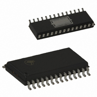
CYWUSB6934-28SEC Cypress Semiconductor Corp, CYWUSB6934-28SEC Datasheet - Page 18

CYWUSB6934-28SEC
Manufacturer Part Number
CYWUSB6934-28SEC
Description
IC WIRELESS USB 2.4GHZ 28-SOIC
Manufacturer
Cypress Semiconductor Corp
Specifications of CYWUSB6934-28SEC
Frequency
2.4GHz
Data Rate - Maximum
62.5kbps
Modulation Or Protocol
DSSS, GFSK
Applications
HID, PC, Peripheral Gaming Devices
Power - Output
0dBm
Sensitivity
-90dBm
Voltage - Supply
2.7 V ~ 3.6 V
Data Interface
PCB, Surface Mount
Antenna Connector
PCB, Surface Mount
Operating Temperature
0°C ~ 70°C
Package / Case
28-SOIC
Operating Temperature (min)
0C
Operating Temperature (max)
70C
Operating Temperature Classification
Commercial
Operating Supply Voltage (min)
2.7V
Operating Supply Voltage (typ)
3V
Operating Supply Voltage (max)
3.6V
Lead Free Status / RoHS Status
Contains lead / RoHS non-compliant
Memory Size
-
Current - Transmitting
-
Current - Receiving
-
Lead Free Status / Rohs Status
Not Compliant
Other names
428-1580-5
Available stocks
Company
Part Number
Manufacturer
Quantity
Price
Company:
Part Number:
CYWUSB6934-28SEC
Manufacturer:
CY
Quantity:
22 751
Table 22. Wake Status
Table 23. Analog Control
Document 38-16007 Rev. *J
7:1
0
7
6
5
4:3
2
1
0
Bit
Bit
Reserved
Reserved
Reg Write Control Enables write access to Reg 0x2E and Reg 0x2F.
MID Read Enable The MID Read Enable bit must be set to read the contents of the Manufacturing ID register (Reg 0x3C-0x3F).
Reserved
PA Output Enable The Power Amplifier Output Enable bit is used to enable the PACTL pin for control of an external power
PA Invert
Reset
Reserved
Wakeup Status Wakeup status.
7
7
Addr: 0x1D
Addr: 0x20
Name
Name
Reg Write
Control
These bits are reserved. This register is read-only.
0 = Wake interrupt not pending
1 = Wake interrupt pending
This IRQ will assert when a wakeup condition occurs. This bit is cleared by reading the Wake Status register
(Reg 0x1D). This register is read-only.
6
6
This bit is reserved and should be written with zero.
1 = Enables write access to Reg 0x2E and Reg 0x2F
0 = Reg 0x2E and Reg 0x2F are read-only
Enabling the Manufacturing ID register (Reg 0x3C-0x3F) consumes power. This bit should only be set when
reading the contents of the Manufacturing ID register (Reg 0x3C-0x3F).
1 = Enables read of MID registers
0 = Disables read of MID registers
These bits are reserved and should be written with zeroes.
amplifier.
1 = PA Control Output Enabled on PACTL pin
0 = PA Control Output Disabled on PACTL pin
The Power Amplifier Invert bit is used to specify the polarity of the PACTL signal when the PA Output Enable
bit is set high. PA Output Enable and PA Invert cannot be simultaneously changed.
1 = PACTL active low
0 = PACTL active high
The Reset bit is used to generate a self-clearing device reset.
1 = Device Reset. All registers are restored to their default values.
0 = No Device Reset.
MID Read
Enable
5
5
Reserved
Reserved
REG_ANALOG_CTL
REG_WAKE_STAT
4
4
Reserved
Description
Description
3
3
PA Output
Enable
2
2
PA Invert
1
1
CYWUSB6934
CYWUSB6932
Default: 0x01
Default: 0x00
Wakeup Status
Page 18 of 33
Reset
0
0
[+] Feedback


