CYWUSB6934-28SEC Cypress Semiconductor Corp, CYWUSB6934-28SEC Datasheet - Page 5
CYWUSB6934-28SEC
Manufacturer Part Number
CYWUSB6934-28SEC
Description
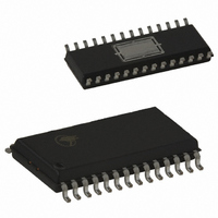
IC WIRELESS USB 2.4GHZ 28-SOIC
Manufacturer
Cypress Semiconductor Corp
Specifications of CYWUSB6934-28SEC
Frequency
2.4GHz
Data Rate - Maximum
62.5kbps
Modulation Or Protocol
DSSS, GFSK
Applications
HID, PC, Peripheral Gaming Devices
Power - Output
0dBm
Sensitivity
-90dBm
Voltage - Supply
2.7 V ~ 3.6 V
Data Interface
PCB, Surface Mount
Antenna Connector
PCB, Surface Mount
Operating Temperature
0°C ~ 70°C
Package / Case
28-SOIC
Operating Temperature (min)
0C
Operating Temperature (max)
70C
Operating Temperature Classification
Commercial
Operating Supply Voltage (min)
2.7V
Operating Supply Voltage (typ)
3V
Operating Supply Voltage (max)
3.6V
Lead Free Status / RoHS Status
Contains lead / RoHS non-compliant
Memory Size
-
Current - Transmitting
-
Current - Receiving
-
Lead Free Status / Rohs Status
Not Compliant
Other names
428-1580-5
Available stocks
Company
Part Number
Manufacturer
Quantity
Price
Company:

Part Number:
CYWUSB6934-28SEC
Manufacturer:
CY
Quantity:
22 751


DIO Interface
The DIO communications interface is an optional SERDES
bypass data-only transfer interface. In receive mode, DIO and
DIOVAL are valid after the falling edge of IRQ, which clocks the
data as shown in
are sampled on the falling edge of the IRQ, which clocks the data
as shown in
DIOVAL on the rising edge of IRQ.
Interrupts
The CYWUSB6932/CYWUSB6934 ICs feature three sets of
interrupts: transmit, receive (CYWUSB6934 only), and a wake
interrupt. These interrupts all share a single pin (IRQ), but can
be independently enabled/disabled. In transmit mode, all receive
interrupts are automatically disabled, and in receive mode all
transmit interrupts are automatically disabled. However, the
contents of the enable registers are preserved when switching
between transmit and receive modes.
Interrupts are enabled and the status read through 6 registers:
Receive Interrupt Enable (Reg 0x07), Receive Interrupt Status
(Reg 0x08), Transmit Interrupt Enable (Reg 0x0D), Transmit
Interrupt Status (Reg 0x0E), Wake Enable (Reg 0x1C), Wake
Status (Reg 0x1D).
If more than 1 interrupt is enabled at any time, it is necessary to
read the relevant interrupt status register to determine which
event caused the IRQ pin to assert. Even when a given interrupt
source is disabled, the status of the condition that would
otherwise cause an interrupt can be determined by reading the
appropriate interrupt status register. It is therefore possible to
use the devices without making use of the IRQ pin at all.
Firmware can poll the interrupt status register(s) to wait for an
event, rather than using the IRQ pin.
The polarity of all interrupts can be set by writing to the Configu-
ration register (Reg 0x05), and it is possible to configure the IRQ
pin to be open drain (if active low) or open source (if active high).
Document 38-16007 Rev. *J
DIOVAL
DIOVAL
IRQ
DIO
IRQ
DIO
Figure
Figure
6. The application MCU samples the DIO and
5. In transmit mode, DIO and DIOVAL
v0
d0
v0
d0
v1
d1
v1
d1
v2
d2
d2
v2
v3
d3
d3
v3
v4
d4
d4
v4
v5
d5
d5
v5
data from mcu
data to mcu
d6
v6
d6
v6
Figure 6. DIO Transmit Sequence
Figure 5. DIO Receive Sequence
v7
d7
v7
d7
d8
v8
v8
d8
d9
v9
v9
d9
d10
v10
v10
d10
v11
d11
v11
d11
d12
v12
d12
v12
Wake Interrupt
When the PD pin is low, the oscillator is stopped. After PD is
deasserted, the oscillator takes time to start, and until it has done
so, it is not safe to use the SPI interface. The wake interrupt
indicates that the oscillator has started, and that the device is
ready to receive SPI transfers.
The wake interrupt is enabled by setting bit 0 of the Wake Enable
register (Reg 0x1C, bit 0=1). Whether or not a wake interrupt is
pending is indicated by the state of bit 0 of the Wake Status
register (Reg 0x1D, bit 0). Reading the Wake Status register
(Reg 0x1D) clears the interrupt.
Transmit Interrupts
Four interrupts are provided to flag the occurrence of transmit
events. The interrupts are enabled by writing to the Transmit
Interrupt Enable register (Reg 0x0D), and their status may be
determined by reading the Transmit Interrupt Status register
(Reg 0x0E). If more than 1 interrupt is enabled, it is necessary to
read the Transmit Interrupt Status register (Reg 0x0E) to
determine which event caused the IRQ pin to assert.
The function and operation of these interrupts are described in
detail in Section .
Receive Interrupts
Eight interrupts are provided to flag the occurrence of receive
events, four each for SERDES A and B. In 64 chips/bit and 32
chips/bit DDR modes, only the SERDES A interrupts are
available, and the SERDES B interrupts will never trigger, even
if enabled. The interrupts are enabled by writing to the Receive
Interrupt Enable register (Reg 0x07), and their status may be
determined by reading the Receive Interrupt Status register (Reg
0x08). If more than one interrupt is enabled, it is necessary to
read the Receive Interrupt Status register (Reg 0x08) to
determine which event caused the IRQ pin to assert.
The function and operation of these interrupts are described in
detail in Section .
d13
v13
d13
v13
d14
v14
v14
d14
d...
v...
v...
d...
CYWUSB6934
CYWUSB6932
Page 5 of 33
[+] Feedback
Related parts for CYWUSB6934-28SEC
Image
Part Number
Description
Manufacturer
Datasheet
Request
R

Part Number:
Description:
IC USB WIRELESS 2.4GHZ 48VQFN
Manufacturer:
Cypress Semiconductor Corp
Datasheet:
Part Number:
Description:
IC WIRELESS USB 2.4GHZ 48VQFN
Manufacturer:
Cypress Semiconductor Corp
Datasheet:

Part Number:
Description:
IC WIRELESS USB 2.4GHZ 48VQFN
Manufacturer:
Cypress Semiconductor Corp
Datasheet:
Part Number:
Description:
Manufacturer:
Cypress Semiconductor Corp
Datasheet:
Part Number:
Description:
Manufacturer:
Cypress Semiconductor Corp
Datasheet:
Part Number:
Description:
Manufacturer:
Cypress Semiconductor Corp
Datasheet:
Part Number:
Description:
Manufacturer:
Cypress Semiconductor Corp
Datasheet: