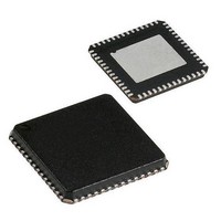
CYRF6936-40LFXC Cypress Semiconductor Corp, CYRF6936-40LFXC Datasheet - Page 3

CYRF6936-40LFXC
Manufacturer Part Number
CYRF6936-40LFXC
Description
IC WIRELESS USB LP 40VQFN
Manufacturer
Cypress Semiconductor Corp
Datasheet
1.CYRF6936-40LFXC.pdf
(23 pages)
Specifications of CYRF6936-40LFXC
Frequency
2.4GHz
Data Rate - Maximum
1Mbps
Modulation Or Protocol
DSSS, GFSK
Applications
Remote Control
Power - Output
4dBm
Sensitivity
-97dBm
Voltage - Supply
1.8 V ~ 3.6 V
Current - Receiving
21.2mA
Current - Transmitting
34mA
Data Interface
PCB, Surface Mount
Antenna Connector
PCB, Surface Mount
Operating Temperature
0°C ~ 70°C
Package / Case
40-VQFN Exposed Pad, 40-HVQFN, 40-SQFN, 40-DHVQFN
Interface
SPI
Termination Type
SMD
Bandwidth
876kHz
Supply Voltage Max
3.6V
Data Rate Max
1000Kbps
Frequency Band Type
ISM
Features
10
Frequency Band Range
2.400 - 2.483 GHz
Supply Voltage Min
2.4V
Lead Free Status / RoHS Status
Lead free / RoHS Compliant
Memory Size
-
Lead Free Status / Rohs Status
Lead free / RoHS Compliant
Other names
428-2024
CYRF6936-40LFXC
CYRF6936-40LFXC
Available stocks
Company
Part Number
Manufacturer
Quantity
Price
Company:
Part Number:
CYRF6936-40LFXC
Manufacturer:
CYPRESS
Quantity:
210
Part Number:
CYRF6936-40LFXC
Manufacturer:
CRIIUS
Quantity:
20 000
Document #: 38-16015 Rev. *H
Table 1. Pin Description (continued)
Functional Overview
The CYRF6936 IC provides a complete WirelessUSB SPI to
antenna wireless MODEMs. The SoC is designed to
implement wireless device links operating in the worldwide
2.4 GHz ISM frequency band. It is intended for systems
compliant with worldwide regulations covered by ETSI EN 301
489-1 V1.41, ETSI EN 300 328-1 V1.3.1 (Europe), FCC CFR
47 Part 15 (USA and Industry Canada), and TELEC
ARIB_T66_March, 2003 (Japan).
The SoC contains a 2.4 GHz, 1 Mbps GFSK radio transceiver,
packet data buffering, packet framer, DSSS baseband
controller, Received Signal Strength Indication (RSSI), and
SPI interface for data transfer and device configuration.
The radio supports 98 discrete 1 MHz channels (regulations
may limit the use of some of these channels in certain jurisdic-
tions).
The baseband performs DSSS spreading/despreading, Start
of Packet (SOP), End of Packet (EOP) detection, and CRC16
generation and checking. The baseband may also be
configured to automatically transmit Acknowledge (ACK)
handshake packets whenever a valid packet is received.
When in receive mode, with packet framing enabled, the
device is always ready to receive data transmitted at any of the
supported bit rates. This enables the implementation of
mixed-rate systems in which different devices use different
data rates. This also enables the implementation of dynamic
data rate systems that use high data rates at shorter distances
or in a low-moderate interference environment or both. It
changes to lower data rates at longer distances or in high inter-
ference environments or both.
In addition, the CYRF6936 IC has a Power Management Unit
(PMU), which enables direct connection of the device to any
battery voltage in the range 1.8V to 3.6V. The PMU conditions
the battery voltage to provide the supply voltages required by
the device, and may supply external devices.
34
35
37
40
E-PAD
Corner Tabs
Pin Number
RST
V
L/D
V
GND
NC
DD
REG
Name
Type
GND
Pwr
Pwr
NC
O
I
Default
I
Device reset. Internal 10 kohm pull down resistor. Active HIGH,
connect through a 0.47 μF capacitor to V
the first time power is applied to the radio. Otherwise the state of the
radio control registers is unknown.
Decoupling pin for 1.8V logic regulator, connect through a 0.47 μF
capacitor to GND.
PMU inductor/diode connection, when used. If not used, connect to
GND.
PMU boosted output voltage feedback.
Must be soldered to Ground.
Do Not solder the tabs and keep other signal traces clear. All tabs are
common to the lead frame or paddle which is grounded after the pad
is grounded. While they are visible to the user, they do not extend to
the bottom.
Data Transmission Modes
The SoC supports four different data transmission modes:
■
■
■
■
Both 64 chip and 32 chip Pseudo Noise (PN) codes are
supported. The four data transmission modes apply to the data
after the SOP. In particular the length, data, and CRC16 are all
sent in the same mode. In general, lower data rates reduce
packet error rate in any given environment.
Link Layer Modes
The CYRF6936 IC device supports the following data packet
framing features:
SOP
Packets begin with a two-symbol SoP marker. This is required
in GFSK and 8DR modes, but is optional in DDR mode and is
not supported in SDR mode. If framing is disabled then an SOP
event is inferred whenever two successive correlations are
detected. The SOP_CODE_ADR code used for the SOP is
different from that used for the “body” of the packet, and if
desired may be a different length. SOP must be configured to
be the same length on both sides of the link.
Length
There are two options for detecting the end of a packet. If SOP
is enabled, then the length field must be enabled. GFSK and
8DR must enable the length field. This is the first eight bits after
the SOP symbol, and is transmitted at the payload data rate.
When the length field is enabled, an EoP condition is inferred
after reception of the number of bytes defined in the length
In GFSK mode, data is transmitted at 1 Mbps, without any
DSSS.
In 8DR mode, eight bits are encoded in each derived code
symbol transmitted.
In DDR mode, two bits are encoded in each derived code
symbol transmitted (As in the CYWUSB6934 DDR mode).
In SDR mode, one bit is encoded in each derived code
symbol transmitted (As in the CYWUSB6934 standard
modes).
Description
BAT.
Must have RST = 1 event
CYRF6936
Page 3 of 23
[+] Feedback


