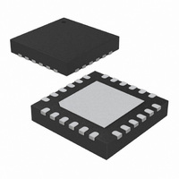
ATA8742-PXQW Atmel, ATA8742-PXQW Datasheet - Page 31

ATA8742-PXQW
Manufacturer Part Number
ATA8742-PXQW
Description
MCU W/TRANSMITTER ASK/FSK 24QFN
Manufacturer
Atmel
Datasheet
1.ATA8742-PXQW.pdf
(238 pages)
Specifications of ATA8742-PXQW
Frequency
433MHz
Applications
Home Automation, Remote Sensing, RKE
Modulation Or Protocol
ASK, FSK
Data Rate - Maximum
32 kBit/s
Power - Output
7.5dBm
Current - Transmitting
9.8mA
Data Interface
PCB, Surface Mount
Antenna Connector
PCB, Surface Mount
Memory Size
4kB Flash, 256B EEPROM, 256B SRAM
Voltage - Supply
2 V ~ 4 V
Operating Temperature
-40°C ~ 85°C
Package / Case
24-VQFN Exposed Pad, 24-HVQFN, 24-SQFN, 24-DHVQFN
Processor Series
ATA8x
Core
AVR8
Data Bus Width
8 bit
Program Memory Type
Flash
Program Memory Size
4 KB
Data Ram Size
256 B
Interface Type
SPI, USI
Maximum Clock Frequency
8.1 MHz
Number Of Programmable I/os
12
Number Of Timers
2
Maximum Operating Temperature
+ 85 C
Mounting Style
SMD/SMT
Development Tools By Supplier
ATASTK512-EK1-IND
Minimum Operating Temperature
- 40 C
On-chip Adc
10 bit, 8 Channel
Lead Free Status / RoHS Status
Lead free / RoHS Compliant
Features
-
Lead Free Status / Rohs Status
Details
Available stocks
Company
Part Number
Manufacturer
Quantity
Price
Company:
Part Number:
ATA8742-PXQW
Manufacturer:
ATMEL
Quantity:
1 482
- Current page: 31 of 238
- Download datasheet (4Mb)
13. Memories
13.1
13.2
9151A–INDCO–07/09
In-System Re-programmable Flash Program Memory
SRAM Data Memory
This section describes the different memories in the ATtiny24/44/84. The AVR architecture has
two main memory spaces, the Data memory and the Program memory space. In addition, the
ATtiny24/44/84 features an EEPROM Memory for data storage. All three memory spaces are lin-
ear and regular.
The ATtiny24/44/84 contains 2/4/8K byte On-chip In-System Reprogrammable Flash memory
for program storage. Since all AVR instructions are 16 or 32 bits wide, the Flash is organized as
1024/2048/4096 x 16.
The Flash memory has an endurance of at least 10,000 write/erase cycles. The ATtiny24/44/84
Program Counter (PC) is 10/11/12 bits wide, thus addressing the 1024/2048/4096 Program
memory locations.
data serial downloading using the SPI pins.
Constant tables can be allocated within the entire Program memory address space (see the
LPM – Load Program memory instruction description).
Timing diagrams for instruction fetch and execution are presented in
ing” on page
Figure 13-1. Program Memory Map
Figure 13-2 on page 32
The lower 160 Data memory locations address both the Register File, the I/O memory and the
internal data SRAM. The first 32 locations address the Register File, the next 64 locations the
standard I/O memory, and the last 128/256/512 locations address the internal data SRAM.
The five different addressing modes for the Data memory cover: Direct, Indirect with Displace-
ment, Indirect, Indirect with Pre-decrement, and Indirect with Post-increment. In the Register
File, registers R26 to R31 feature the indirect addressing pointer registers.
The direct addressing reaches the entire data space.
The Indirect with Displacement mode reaches 63 address locations from the base address given
by the Y- or Z-register.
28.
“Memory Programming” on page 180
shows how the ATtiny24/44/84 SRAM Memory is organized.
Program Memory
0x03FF/0x07FF/0xFFF
0x0000
contains a detailed description on Flash
“Instruction Execution Tim-
ATA8742
31
Related parts for ATA8742-PXQW
Image
Part Number
Description
Manufacturer
Datasheet
Request
R

Part Number:
Description:
Manufacturer:
ATMEL Corporation
Datasheet:

Part Number:
Description:
DEV KIT FOR AVR/AVR32
Manufacturer:
Atmel
Datasheet:

Part Number:
Description:
INTERVAL AND WIPE/WASH WIPER CONTROL IC WITH DELAY
Manufacturer:
ATMEL Corporation
Datasheet:

Part Number:
Description:
Low-Voltage Voice-Switched IC for Hands-Free Operation
Manufacturer:
ATMEL Corporation
Datasheet:

Part Number:
Description:
MONOLITHIC INTEGRATED FEATUREPHONE CIRCUIT
Manufacturer:
ATMEL Corporation
Datasheet:

Part Number:
Description:
AM-FM Receiver IC U4255BM-M
Manufacturer:
ATMEL Corporation
Datasheet:

Part Number:
Description:
Monolithic Integrated Feature Phone Circuit
Manufacturer:
ATMEL Corporation
Datasheet:

Part Number:
Description:
Multistandard Video-IF and Quasi Parallel Sound Processing
Manufacturer:
ATMEL Corporation
Datasheet:

Part Number:
Description:
High-performance EE PLD
Manufacturer:
ATMEL Corporation
Datasheet:

Part Number:
Description:
8-bit Flash Microcontroller
Manufacturer:
ATMEL Corporation
Datasheet:

Part Number:
Description:
2-Wire Serial EEPROM
Manufacturer:
ATMEL Corporation
Datasheet:


