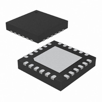
ATA8742-PXQW Atmel, ATA8742-PXQW Datasheet - Page 91

ATA8742-PXQW
Manufacturer Part Number
ATA8742-PXQW
Description
MCU W/TRANSMITTER ASK/FSK 24QFN
Manufacturer
Atmel
Datasheet
1.ATA8742-PXQW.pdf
(238 pages)
Specifications of ATA8742-PXQW
Frequency
433MHz
Applications
Home Automation, Remote Sensing, RKE
Modulation Or Protocol
ASK, FSK
Data Rate - Maximum
32 kBit/s
Power - Output
7.5dBm
Current - Transmitting
9.8mA
Data Interface
PCB, Surface Mount
Antenna Connector
PCB, Surface Mount
Memory Size
4kB Flash, 256B EEPROM, 256B SRAM
Voltage - Supply
2 V ~ 4 V
Operating Temperature
-40°C ~ 85°C
Package / Case
24-VQFN Exposed Pad, 24-HVQFN, 24-SQFN, 24-DHVQFN
Processor Series
ATA8x
Core
AVR8
Data Bus Width
8 bit
Program Memory Type
Flash
Program Memory Size
4 KB
Data Ram Size
256 B
Interface Type
SPI, USI
Maximum Clock Frequency
8.1 MHz
Number Of Programmable I/os
12
Number Of Timers
2
Maximum Operating Temperature
+ 85 C
Mounting Style
SMD/SMT
Development Tools By Supplier
ATASTK512-EK1-IND
Minimum Operating Temperature
- 40 C
On-chip Adc
10 bit, 8 Channel
Lead Free Status / RoHS Status
Lead free / RoHS Compliant
Features
-
Lead Free Status / Rohs Status
Details
Available stocks
Company
Part Number
Manufacturer
Quantity
Price
Company:
Part Number:
ATA8742-PXQW
Manufacturer:
ATMEL
Quantity:
1 482
- Current page: 91 of 238
- Download datasheet (4Mb)
20.5
9151A–INDCO–07/09
Output Compare Unit
Signal description (internal signals):
Depending of the mode of operation used, the counter is cleared, incremented, or decremented
at each timer clock (clk
selected by the Clock Select bits (CS02:0). When no clock source is selected (CS02:0 = 0) the
timer is stopped. However, the TCNT0 value can be accessed by the CPU, regardless of
whether clk
count operations.
The counting sequence is determined by the setting of the WGM01 and WGM00 bits located in
the Timer/Counter Control Register (TCCR0A) and the WGM02 bit located in the Timer/Counter
Control Register B (TCCR0B). There are close connections between how the counter behaves
(counts) and how waveforms are generated on the Output Compare output OC0A. For more
details about advanced counting sequences and waveform generation, see
tion” on page
The Timer/Counter Overflow Flag (TOV0) is set according to the mode of operation selected by
the WGM01:0 bits. TOV0 can be used for generating a CPU interrupt.
The 8-bit comparator continuously compares TCNT0 with the Output Compare Registers
(OCR0A and OCR0B). Whenever TCNT0 equals OCR0A or OCR0B, the comparator signals a
match. A match will set the Output Compare Flag (OCF0A or OCF0B) at the next timer clock
cycle. If the corresponding interrupt is enabled, the Output Compare Flag generates an Output
Compare interrupt. The Output Compare Flag is automatically cleared when the interrupt is exe-
cuted. Alternatively, the flag can be cleared by software by writing a logical one to its I/O bit
location. The Waveform Generator uses the match signal to generate an output according to
operating mode set by the WGM02:0 bits and Compare Output mode (COM0x1:0) bits. The max
and bottom signals are used by the Waveform Generator for handling the special cases of the
extreme values in some modes of operation. See
Figure 20-3 on page 92
count
direction
clear
clk
top
bottom
Tn
T0
94.
is present or not. A CPU write overrides (has priority over) all counter clear or
T0
shows a block diagram of the Output Compare unit.
). clk
Increment or decrement TCNT0 by 1.
Select between increment and decrement.
Clear TCNT0 (set all bits to zero).
Timer/Counter clock, referred to as clk
Signalize that TCNT0 has reached maximum value.
Signalize that TCNT0 has reached minimum value (zero).
T0
can be generated from an external or internal clock source,
“Modes of Operation” on page
T0
in the following.
“Modes of Opera-
ATA8742
94.
91
Related parts for ATA8742-PXQW
Image
Part Number
Description
Manufacturer
Datasheet
Request
R

Part Number:
Description:
Manufacturer:
ATMEL Corporation
Datasheet:

Part Number:
Description:
DEV KIT FOR AVR/AVR32
Manufacturer:
Atmel
Datasheet:

Part Number:
Description:
INTERVAL AND WIPE/WASH WIPER CONTROL IC WITH DELAY
Manufacturer:
ATMEL Corporation
Datasheet:

Part Number:
Description:
Low-Voltage Voice-Switched IC for Hands-Free Operation
Manufacturer:
ATMEL Corporation
Datasheet:

Part Number:
Description:
MONOLITHIC INTEGRATED FEATUREPHONE CIRCUIT
Manufacturer:
ATMEL Corporation
Datasheet:

Part Number:
Description:
AM-FM Receiver IC U4255BM-M
Manufacturer:
ATMEL Corporation
Datasheet:

Part Number:
Description:
Monolithic Integrated Feature Phone Circuit
Manufacturer:
ATMEL Corporation
Datasheet:

Part Number:
Description:
Multistandard Video-IF and Quasi Parallel Sound Processing
Manufacturer:
ATMEL Corporation
Datasheet:

Part Number:
Description:
High-performance EE PLD
Manufacturer:
ATMEL Corporation
Datasheet:

Part Number:
Description:
8-bit Flash Microcontroller
Manufacturer:
ATMEL Corporation
Datasheet:

Part Number:
Description:
2-Wire Serial EEPROM
Manufacturer:
ATMEL Corporation
Datasheet:


