CM100DY-24NF Powerex Inc, CM100DY-24NF Datasheet - Page 2
CM100DY-24NF
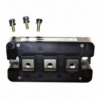
Manufacturer Part Number
CM100DY-24NF
Description
IGBT MOD DUAL 1200V 100A NF SER
Manufacturer
Powerex Inc
Series
IGBTMOD™r
Type
IGBT Moduler
Datasheet
1.CM100DY-24NF.pdf
(4 pages)
Specifications of CM100DY-24NF
Configuration
Half Bridge
Voltage - Collector Emitter Breakdown (max)
1200V
Vce(on) (max) @ Vge, Ic
2.5V @ 15V, 100A
Current - Collector (ic) (max)
100A
Current - Collector Cutoff (max)
1mA
Input Capacitance (cies) @ Vce
23nF @ 10V
Power - Max
650W
Input
Standard
Ntc Thermistor
No
Mounting Type
Chassis Mount
Package / Case
Module
Distributorinventory
View
Voltage
1200V
Current
100A
Circuit Configuration
Dual
Rohs Compliant
Yes
Recommended Gate Driver
VLA504
Recommended Dc To Dc Converter
VLA106-15242 or VLA106-24242
Interface Circuit Ref Design
BG2B-3015
For Use With
BG2B-5015 - KIT DEV BOARD 2CN 5A FOR IGBTBG2B-3015 - KIT DEV BOARD 2CN 3A FOR IGBTBG2B-1515 - KIT DEV BOARD 1.5A FOR IGBTBG2A-NF - KIT DEV BOARD FOR IGBT
Lead Free Status / RoHS Status
Lead free / RoHS Compliant
Igbt Type
-
Other names
835-1006
Available stocks
Company
Part Number
Manufacturer
Quantity
Price
Company:

Part Number:
CM100DY-24NF
Manufacturer:
Powerex Inc
Quantity:
135
Part Number:
CM100DY-24NF
Manufacturer:
MITSUBISHI/三菱
Quantity:
20 000
Part Number:
CM100DY-24NF
Quantity:
55


2
Powerex, Inc., 200 E. Hillis Street, Youngwood, Pennsylvania 15697-1800 (724) 925-7272
CM100DY-24NF
Dual IGBTMOD™ NF-Series Module
100 Amperes/1200 Volts
Absolute Maximum Ratings, T
Ratings
Junction Temperature
Storage Temperature
Collector-Emitter Voltage (G-E Short)
Gate-Emitter Voltage (C-E Short)
Collector Current*** (DC, T
Peak Collector Current
Emitter Current** (T
Peak Emitter Current**
Maximum Collector Dissipation (T
Mounting Torque, M5 Main Terminal
Mounting Torque, M6 Mounting
Weight
Isolation Voltage (Main Terminal to Baseplate, AC 1 min.)
Static Electrical Characteristics, T
Characteristics
Collector-Cutoff Current
Gate Leakage Current
Gate-Emitter Threshold Voltage
Collector-Emitter Saturation Voltage
Total Gate Charge
Emitter-Collector Voltage**
Dynamic Electrical Characteristics, T
Characteristics
Input Capacitance
Output Capacitance
Reverse Transfer Capacitance
Inductive
Load
Switch
Time
Diode Reverse Recovery Time**
Diode Reverse Recovery Charge**
*Pulse width and repetition rate should be such that device junction temperature (T
**Represents characteristics of the anti-parallel, emitter-to-collector free-wheel diode (FWDi).
***Tc' measured point is just under the chips. If this value is used, Rth(f-a) should be measured just under the chips
C
= 25 C)
Turn-on Delay Time
Rise Time
Turn-off Delay Time
Fall Time
C
' = 113 C)
C
= 25 C, T
j
= 25 C unless otherwise specified
j
j
= 25 C unless otherwise specified
V
V
Symbol
Symbol
CE(sat)
150 C)
t
t
I
I
C
GE(th)
C
V
C
d(on)
d(off)
GES
CES
Q
j
Q
t
oes
EC
t
ies
res
t
= 25 C unless otherwise specified
rr
r
f
G
rr
V
I
I
C
CC
V
C
GE1
= 100A, V
= 100A, V
= 600V, I
V
V
V
I
C
V
I
CC
Switching Operation,
CE
GE
= V
E
CE
= 10mA, V
= 100A, V
Inductive Load
Test Conditions
Test Conditions
= V
= 600V, I
= V
GE2
j
) does not exceed T
= 10V, V
I
E
GE
C
GE
CES
GES
= 100A
= 15V, R
= 100A, V
= 15V, T
= 15V, T
, V
, V
CE
C
GE
GE
GE
CE
= 100A,
= 10V
= 0V
= 0V
G
= 0V
= 0V
j
j
GE
= 125 C
= 3.1 ,
= 25 C
Symbol
V
V
V
T
I
j(max)
I
= 15V
GES
P
CES
CM
EM
—
—
—
T
I
ISO
I
stg
E
C
C
j
rating.
Min.
Min.
6.0
—
—
—
—
—
—
—
—
—
—
—
—
—
—
—
CM100DY-24NF
–40 to 150
–40 to 125
1200
2500
200*
200*
100
650
310
100
30
40
20
Typ.
Typ.
675
7.0
1.8
2.0
5.0
—
—
—
—
—
—
—
—
—
—
—
Max.
Max.
120
450
350
150
1.0
0.5
8.0
2.5
3.2
—
—
—
23
80
2
0.45
Amperes
Amperes
Amperes
Amperes
Grams
Watts
Volts
Volts
Volts
Units
in-lb
in-lb
Volts
Volts
Volts
Volts
Units
Units
C
C
mA
nC
ns
ns
ns
ns
ns
nf
nf
nf
A
C
Related parts for CM100DY-24NF
Image
Part Number
Description
Manufacturer
Datasheet
Request
R

Part Number:
Description:
IGBT MOD DUAL 600V 100A H SER
Manufacturer:
Powerex Inc
Datasheet:
Part Number:
Description:
IGBT MOD DUAL 1200V 100A H SER
Manufacturer:
Powerex Inc
Datasheet:

Part Number:
Description:
IGBT MOD DUAL 1200V 100A A SER
Manufacturer:
Powerex Inc
Datasheet:

Part Number:
Description:
SINGLE IGBTMOD(TM) TRANSISTOR MODULES DUAL IGBTMOD TRANSISTOR MODULES
Manufacturer:
Powerex Inc
Part Number:
Description:
IGBT MODULE A-SERIES DUAL DP 1700 100
Manufacturer:
Powerex Inc
Datasheet:
Part Number:
Description:
TRANSISTOR,IGBT POWER MODULE,HALF BRIDGE,1.4kV V(BR)CES,100A I(C)
Manufacturer:
Powerex Inc
Datasheet:


Part Number:
Description:
Ethernet Modules & Development Tools Cobox Mini Device Server 10/100 2-TTL
Manufacturer:
Lantronix
Datasheet:

Part Number:
Description:
Switch Fabric, Tilt Switch - Metal - Mercury Contacts
Manufacturer:
Comus Group of Companies
Part Number:
Description:
Switch Fabric, Tilt Modules
Manufacturer:
Comus Group of Companies
Part Number:
Description:
Manufacturer:
Powerex Inc
Datasheet:
Part Number:
Description:
Manufacturer:
Powerex Inc
Datasheet: