CPV363M4F Vishay, CPV363M4F Datasheet
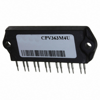
CPV363M4F
Specifications of CPV363M4F
VS-CPV363M4F
VS-CPV363M4F
VSCPV363M4F
VSCPV363M4F
Available stocks


Related parts for CPV363M4F

CPV363M4F Summary of contents
Page 1
... R (IGBT) Junction-to-Case, each IGBT, one IGBT in conduction JC R (DIODE) Junction-to-Case, each diode, one diode in conduction JC R (MODULE) Case-to-Sink, flat, greased surface CS Wt Weight of module CPV363M4F 90° 125°C, Supply Voltage 360Vdc -40 to +150 300 (0.063 in. (1.6mm) from case) 5-7 lbf•in (0.55-0.8 N•m) ...
Page 2
... CPV363M4F Electrical Characteristics @ T Parameter V Collector-to-Emitter Breakdown Voltage (BR)CES Temperature Coeff. of Breakdown Voltage (BR)CES J V Collector-to-Emitter Saturation Voltage CE(on) V Gate Threshold Voltage GE(th Temperature Coeff. of Threshold Voltage ––– GE(th Forward Transconductance fe I Zero Gate Voltage Collector Current CES V Diode Forward Voltage Drop ...
Page 3
... 20µs PULSE WIDTH Collector-to-Emitter Voltage ( Fig Typical Output Characteristics 1 f, Frequency (KHz) (Load Current = I of fundamental) RMS 15V Fig Typical Transfer Characteristics CPV363M4F 0° ° tor = ula tio . ted V o lta 150° 25° 5µs PULSE WIDTH Gate-to-Emitter Voltage ( 4.10 3.51 2 ...
Page 4
... CPV363M4F Case Temperature ( C Fig Maximum Collector Current vs. Case Temperature 0.50 1 0.20 0.10 0.05 0. 0.01 SINGLE PULSE ( THE RMAL RES PO NSE) 0.01 0.0000 1 0.0001 Fig Maximum Effective Transient Thermal Impedance, Junction-to-Case 100 125 150 ° C) Fig Typical Collector-to-Emitter Voltage 0.001 0 ulse D ura tion ( ...
Page 5
... Fig Typical Capacitance vs. Collector-to-Emitter Voltage 0. 480V 15V GE ° 8.7A 0.88 C 0.86 0.84 0.82 0. Gate Resistance (Ohm) G Fig Typical Switching Losses vs. Gate Resistance f = 1MHz C SHORTED 100 CPV363M4F 400V 8. Total Gate Charge (nC) G Fig Typical Gate Charge vs. Gate-to-Emitter Voltage 22Ohm 15V 480V CC 1 0.1 -60 -40 - ...
Page 6
... CPV363M4F 4 Ohm 22 G ° 150 480V 15V GE 3.0 2.0 1.0 0 Collector-to-emitter Current (A) C Fig Typical Switching Losses vs. Collector-to-Emitter Current Fig Maximum Forward Voltage Drop vs. Instantaneous Forward Current 150 ° 125 ° ° orwa rd V olta ge D rop - V 100 V = 20V 125 SAFE OPERATING AREA ...
Page 7
... / /µs) f Fig Typical Reverse Recovery vs ° ° 6 /dt - (A/ µs) f Fig Typical Stored Charge vs ° ° 6 Fig Typical Recovery Current vs /dt f CPV363M4F ° ° 6. / µ ° ° 6 / /µs) f Fig Typical di /dt vs. di (rec / /dt f ...
Page 8
... CPV363M4F 430µF 80% of Vce Fig. 18a - Test Circuit for Measurement off(diode ATE VO LTA . 10 td( on Fig. 18c - Test Waveforms for Circuit of Fig. 18a, Defining Same t ype device as D.U.T. D.U. d(on) r d(off) f Fig. 18b - +V g DUT V O LTA URR E NT Ipk Ic t2 ...
Page 9
... V 60 00µ F 100 ATE D.U. 480V CPV363M4F DE VICE UNDE CURR . D.U.T. CURR 480V @25°C C ...
Page 10
... CPV363M4F Repetitive rating: V =20V; pulse width limited by maximum junction temperature (figure 20 =80%( =20V, L=10µ CES GE Pulse width 80µs; duty factor Pulse width 5.0µs, single shot. 3.91 ( .154) 2X 21.97 (.865 3.94 (.155) 4.06 ± 0.51 (.160 ± .020) 5.08 (.200) 6X WORLD HEADQUARTERS: 233 Kansas St ...