STE70NM60 STMicroelectronics, STE70NM60 Datasheet
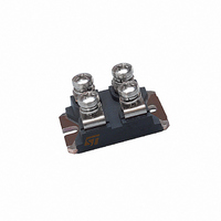
MOSFET N-CH 600V 70A ISOTOP

STE70NM60

Manufacturer Part Number
STE70NM60
Description
MOSFET N-CH 600V 70A ISOTOP
Manufacturer
STMicroelectronics
Series
MDmesh™r
Datasheet

Specifications of STE70NM60

Fet Type
MOSFET N-Channel, Metal Oxide
Fet Feature
Standard
Rds On (max) @ Id, Vgs
55 mOhm @ 30A, 10V
Drain To Source Voltage (vdss)
600V
Current - Continuous Drain (id) @ 25° C
70A
Vgs(th) (max) @ Id
5V @ 250µA
Gate Charge (qg) @ Vgs
266nC @ 10V
Input Capacitance (ciss) @ Vds
7300pF @ 25V
Power - Max
600W
Mounting Type
Chassis Mount
Package / Case
ISOTOP
Transistor Polarity
N Channel
Continuous Drain Current Id
30A
Drain Source Voltage Vds
600V
On Resistance Rds(on)
50mohm
Rds(on) Test Voltage Vgs
10V
Threshold Voltage Vgs Typ
4V
Rohs Compliant
Yes
Configuration
Single Dual Source
Resistance Drain-source Rds (on)
0.055 Ohms
Forward Transconductance Gfs (max / Min)
35 S
Drain-source Breakdown Voltage
600 V
Gate-source Breakdown Voltage
+/- 30 V
Continuous Drain Current
70 A
Power Dissipation
600 W
Maximum Operating Temperature
+ 150 C
Mounting Style
Through Hole
Minimum Operating Temperature
- 65 C
Lead Free Status / RoHS Status
Lead free / RoHS Compliant
Other names
497-3173-5

Available stocks

Company
Part Number
Manufacturer
Quantity
Price
Part Number:
STE70NM60
Manufacturer:
VICOR
Quantity:
1 000
Part Number:
STE70NM60
Manufacturer:
ST
0
Part Number:
STE70NM60
Quantity:
216
DESCRIPTION
The MDmesh™ is a new revolutionary MOSFET
technology that associates the Multiple Drain pro-
cess with the Company’s PowerMESH™ horizontal
layout. The resulting product has an outstanding low
on-resistance, impressively high dv/dt and excellent
avalanche characteristics. The adoption of the
Company’s proprietary strip technique yields overall
dynamic performance that is significantly better than
that of similar competition’s products.
APPLICATIONS
The MDmesh™ family is very suitable for increasing
power density of high voltage converters allowing
system miniaturization and higher efficiencies.
ORDERING INFORMATION
March 2003
STE70NM60
TYPICAL R
HIGH dv/dt AND AVALANCHE CAPABILITIES
IMPROVED ESD CAPABILITY
LOW INPUT CAPACITANCE AND GATE
CHARGE
LOW GATE INPUT RESISTANCE
TIGHT PROCESS CONTROL
INDUSTRY’S LOWEST ON-RESISTANCE
TYPE
SALES TYPE
STE70NM60
DS
(on) = 0.050
V
600V
DSS
< 0.055
R
MARKING
Zener-Protected MDmesh™Power MOSFET
E70NM60
DS(on)
N-CHANNEL 600V - 0.050 - 70A ISOTOP
70 A
I
D
PACKAGE
ISOTOP
INTERNAL SCHEMATIC DIAGRAM
ISOTOP
STE70NM60
PACKAGING
TUBE
1/8

Related parts for STE70NM60

STE70NM60 Summary of contents

Page 1

... ORDERING INFORMATION SALES TYPE STE70NM60 March 2003 N-CHANNEL 600V - 0.050 - 70A ISOTOP Zener-Protected MDmesh™Power MOSFET R I DS(on MARKING PACKAGE E70NM60 ISOTOP STE70NM60 ISOTOP INTERNAL SCHEMATIC DIAGRAM PACKAGING TUBE 1/8 ...

Page 2

... STE70NM60 ABSOLUTE MAXIMUM RATINGS Symbol V Drain-source Voltage ( Drain-gate Voltage (R DGR V Gate- source Voltage GS I Drain Current (continuous Drain Current (continuous Drain Current (pulsed Total Dissipation at T TOT V Gate source ESD(HBM-C=100pF, R=15K ESD(G-S) Derating Factor dv/dt (1) Peak Diode Recovery voltage slope T Storage Temperature ...

Page 3

... V GS Test Conditions V = 400 4 (see test circuit, Figure 5) Test Conditions di/dt = 100 A/µ 150° (see test circuit, Figure 5) STE70NM60 Min. Typ. Max. 600 10 = 125°C 100 ± 0.050 0.055 Min. Typ. Max 7300 GS 2000 40 1.8 Min. Typ. Max 178 266 44.5 95 Min ...

Page 4

... STE70NM60 Safe Operating Area Output Characteristics Transconductance 4/8 Thermal Impedance Transfer Characteristics Static Drain-source On Resistance ...

Page 5

... Gate Charge vs Gate-source Voltage Normalized Gate Threshold Voltage vs Temp. Source-drain Diode Forward Characteristics Capacitance Variations Normalized On Resistance vs Temperature Normalized BVDSS vs Temperature STE70NM60 5/8 ...

Page 6

... STE70NM60 Fig. 1: Unclamped Inductive Load Test Circuit Fig. 3: Switching Times Test Circuit For Resistive Load Fig. 5: Test Circuit For Inductive Load Switching And Diode Recovery Times 6/8 Fig. 2: Unclamped Inductive Waveform Fig. 4: Gate Charge test Circuit ...

Page 7

... STE70NM60 MAX. 0.480 0.358 0.080 0.033 0.503 1.003 1.248 0.169 0.594 1.193 1.503 0.322 7/8 ...

Page 8

... STE70NM60 Information furnished is believed to be accurate and reliable. However, STMicroelectronics assumes no responsibility for the consequences of use of such information nor for any infringement of patents or other rights of third parties which may result from its use. No license is granted by implication or otherwise under any patent or patent rights of STMicroelectronics. Specifications mentioned in this publication are subject to change without notice ...

Related keywords