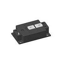
VMO1200-01F IXYS, VMO1200-01F Datasheet
Manufacturer Part Number
VMO1200-01F
Description
MOSFET N-CH 100V 1245A Y3-LI
Type
Single Switch MOSFETs Moduler
Specifications of VMO1200-01F
Fet Type
MOSFET N-Channel, Metal Oxide
Fet Feature
Standard
Rds On (max) @ Id, Vgs
1.35 mOhm @ 932A, 10V
Drain To Source Voltage (vdss)
100V
Current - Continuous Drain (id) @ 25° C
1245A
Vgs(th) (max) @ Id
4V @ 64mA
Gate Charge (qg) @ Vgs
2520nC @ 10V
Mounting Type
Chassis Mount
Package / Case
Y3-Li
Mounting Style
Screw
Product
Power Semiconductor Modules
Typical Delay Time
360 ns
Vdss, Max, (v)
100
Id25, Tc = 25°c, (a)
1220
Id80, Tc = 80°c, (a)
970
Rds(on), Max, Tj = 25°c, (mohms)
1.25
Tf, Typ, (ns)
1020
Tr, Typ, (ns)
1620
Rthjc, Max, (k/w)
0.053
Package Style
Y3-Li (w/o terminal 1, low inductance)
Lead Free Status / RoHS Status
Lead free / RoHS Compliant
Power - Max
-
Lead Free Status / Rohs Status
Lead free / RoHS Compliant
N-Channel Enhancement Mode
PolarHT™ Module
© 2010 IXYS All rights reserved
MOSFET
Symbol
V
V
I
I
I
I
Symbol
R
V
I
I
Q
Q
Q
t
t
t
t
E
E
E
t
t
t
t
E
E
E
R
R
DSS
GSS
D25
D80
F25
F80
d(on)
r
d(off)
f
d(on)
r
d(off)
f
GS(th)
GS
on
off
rec
on
off
rec
DSS
DSon
thJC
thJH
g
gs
gd
Conditions
T
T
T
T
T
Conditions
V
V
V
V
V
inductive load
V
I
R
inductive load
V
I
R
with heat transfer paste (IXYS test setup)
D
D
VJ
C
C
C
C
GS
DS
DS
GS
GS
GS
GS
G
G
= 1000 A; R
= 1000 A; R
= 25°C
= 80°C
= 25°C (diode)
= 80°C (diode)
= R
= R
= 25°C to 150°C
= 0.8 • V
= 10 V; I
= 20 V; I
= ± 20 V; V
= 10 V; V
= 10 V; V
= 10 V; V
G ext
G ext
+ R
+ R
D
D
DSS
DS
DS
DS
= I
= 3 mA
G
G
out driver
out driver
DS
; V
= 50 V; I
= 50 V
= 50 V
= 1.8 Ω
= 1.8 Ω
D80
= 0 V
GS
= 0 V; T
D
= 1000 A
T
T
T
T
T
VJ
VJ
VJ
VJ
VJ
VJ
(T
= 25°C
= 125°C
= 25°C
= 125°C
= 25°C
= 125°C
VJ
= 25°C, unless otherwise specified)
min.
3
Characteristic Values
0.065
1710
1020
1620
1020
1640
Maximum Ratings
1.00
1.62
62.3
0.57
58.9
0.82
typ.
396
360
460
400
560
820
7.7
8.5
G
KS
0.053
0.088
1220
1220
max.
1.25
2.00
± 20
100
970
970
0.3
1.2
5
6
D
S
K/W
K/W
mΩ
mΩ
mA
mA
mJ
mJ
mJ
mJ
mJ
mJ
nC
nC
nC
µA
ns
ns
ns
ns
ns
ns
ns
ns
V
V
A
A
A
A
V
V
I
R
Features
• PolarHT™ MOSFET technology
• package
Applications
• converters with high power density for
D25
- low R
- dv/dt ruggedness
- fast intrinsic reverse diode
- low inductive current path
- screw connection to high current
- use of non interchangeable
- Kelvin source terminals for easy drive
- isolated DCB ceramic base plate
- main and auxiliary AC drives of
- DC drives
- power supplies
DSS
DS(on)
main terminals
connectors for auxiliary terminals
possible
electric vehicles
KS
G
DSon
= 100 V
= 1220 A
= 1.25 mΩ
VMO 1200-01F
S
D
max.
20100614b
1 - 6
Related parts for VMO1200-01F
VMO1200-01F Summary of contents
... I = 1000 ext out driver off E rec R thJC R with heat transfer paste (IXYS test setup) thJH © 2010 IXYS All rights reserved G KS Maximum Ratings ± 20 1220 1220 Characteristic Values (T = 25°C, unless otherwise specified) VJ min. typ. max 25°C 1.00 1.25 ...
... V I < 1 mA, 50/60 Hz ISOL ISOL M Mounting torque (M6) d Terminal connection torque (M6) Weight Product Marking Marking on Ordering Part Name Product Standard VMO1200-01F VMO1200-01F © 2010 IXYS All rights reserved Characteristic Values min. typ. max 25°C 1. 125°C 0.96 VJ 300 T = 25° ...
... Optional accessories for modules keyed twin plugs (UL758, style 1385, CSA class 5851, guide 460-1-1) • Type ZY180L with wire length 350mm - for pins 4 (Gate, yellow wire) and 5 (Kelvin Source, red wire) © 2010 IXYS All rights reserved Dimensions 0.0394“) VMO 1200-01F 20100614b ...
... Fig. 3 Typical output characteristic 2.0 1.6 R DS(on) normalized 1.2 R DS(on) 0.8 normal. 0.4 0.0 -50 - [°C] VJ Fig. 5 Typ. drain source on-state resistance R versus junction temperature T DS(on) © 2010 IXYS All rights reserved 120 160 25° 4.0 3.2 2.4 R DS(on) [mΩ] 1.6 R DS(on) 0.8 0.0 75 ...
... Fig. 8 Typ. turn-on energy & switching times vs. gate resistor, inductive switching 1000 25° [ 400 800 1200 Q [nC] G Fig. 10 Typical gate charge characteristic © 2010 IXYS All rights reserved 1600 100 1200 off 800 [ns] [mJ d(on) 400 800 1000 3000 90 85 2500 t ...
... F Fig. 14 Typical reverse recovery charge Q of the body diode versus di/dt 0.07 0.06 0.05 0.04 0.03 0.02 0.01 0. 100 t [ms] Fig. 16 Typ. transient thermal impedance with heat tranfer paste (IXYS test setup) 600 700 rr 1000 10000 20100614b ...
Related keywords
- VMO1200-01F datasheet
- VMO1200-01F data sheet
- VMO1200-01F pdf datasheet
- VMO1200-01F component
- VMO1200-01F part
- VMO1200-01F distributor
- VMO1200-01F RoHS
- VMO1200-01F datasheet download