NSR20F20NXT5G ON Semiconductor, NSR20F20NXT5G Datasheet
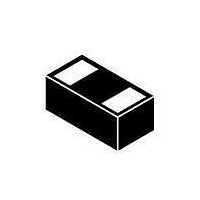
IC DIODE SFC SCHOTTKY 0603 2DSN

NSR20F20NXT5G

Manufacturer Part Number
NSR20F20NXT5G
Description
IC DIODE SFC SCHOTTKY 0603 2DSN
Manufacturer
ON Semiconductor
Datasheet

Specifications of NSR20F20NXT5G

Voltage - Forward (vf) (max) @ If
470mV @ 2A
Voltage - Dc Reverse (vr) (max)
20V
Current - Average Rectified (io)
2A (DC)
Current - Reverse Leakage @ Vr
150µA @ 20V
Diode Type
Schottky
Speed
Fast Recovery =< 500ns, > 200mA (Io)
Mounting Type
Surface Mount
Package / Case
2-DSN
Product
Schottky Diodes
Peak Reverse Voltage
20 V
Forward Continuous Current
2 A
Max Surge Current
28 A
Forward Voltage Drop
450 mV
Maximum Reverse Leakage Current
30 uA
Maximum Power Dissipation
1.56 W
Mounting Style
SMD/SMT
Lead Free Status / RoHS Status
Lead free / RoHS Compliant
Reverse Recovery Time (trr)
-
Capacitance @ Vr, F
-
Lead Free Status / Rohs Status
Lead free / RoHS Compliant
Other names
NSR20F20NXT5G
NSR20F20NXT5GOSTR

Available stocks

Company
Part Number
Manufacturer
Quantity
Price
Part Number:
NSR20F20NXT5G
Manufacturer:
ON
Quantity:
5 000
Part Number:
NSR20F20NXT5G
Manufacturer:
ON Semiconductor
Quantity:
5
Part Number:
NSR20F20NXT5G
Manufacturer:
ZILOG
Quantity:
17
Part Number:
NSR20F20NXT5G
Manufacturer:
ON/安森美
Quantity:
20 000
NSR20F20NXT5G
Schottky Barrier Diode
voltage drop and low leakage current and are offered in a Chip Scale
Package (CSP) to reduce board space. The low thermal resistance
enables designers to meet the challenging task of achieving higher
efficiency and meeting reduced space requirements.
Features
Typical Applications
Markets
Stresses exceeding Maximum Ratings may damage the device. Maximum
Ratings are stress ratings only. Functional operation above the Recommended
Operating Conditions is not implied. Extended exposure to stresses above the
Recommended Operating Conditions may affect device reliability.
MAXIMUM RATINGS
© Semiconductor Components Industries, LLC, 2010
July, 2010 − Rev. 1
Reverse Voltage
Forward Current (DC)
Forward Surge Current (60 Hz @ 1 cycle)
ESD Rating:
These Schottky barrier diodes are optimized for low forward
ESD Rating
Compliant
Low Forward Voltage Drop − 450 mV @ 2.0 A
Low Reverse Current − 30 mA @ 10 V VR
2.0 A of Continuous Forward Current
Power Dissipation of 665 mW with Minimum Trace
ESD Rating − Human Body Model: Class 3B
High Switching Speed
These Devices are Pb−Free, Halogen Free/BFR Free and are RoHS
LCD and Keypad Backlighting
Camera Photo Flash
Buck and Boost dc−dc Converters
Reverse Voltage and Current Protection
Clamping & Protection
Mobile Handsets
MP3 Players
Digital Camera and Camcorders
Notebook PCs & PDAs
GPS
− Machine Model: Class C
Rating
Human Body Model
Machine Model
Symbol
ESD
I
FSM
V
I
F
R
Value
> 400
2.0
> 8
20
28
1
Unit
kV
V
A
A
V
†For information on tape and reel specifications,
NSR20F20NXT5G
including part orientation and tape sizes, please
refer to our Tape and Reel Packaging Specifications
Brochure, BRD8011/D.
CASE 152AB
Device
2
(0603)
DSN2
20F20
YYY
ORDERING INFORMATION
BARRIER DIODE
20 V SCHOTTKY
CATHODE
http://onsemi.com
1
1
= Specific Device Code
= Year Code
(Pb−Free)
Package
DSN2
Publication Order Number:
ANODE
2
5000 / Tape & Reel
MARKING
DIAGRAM
PIN 1
Shipping†
20F20
NSR20F20/D
YYY

Related parts for NSR20F20NXT5G

NSR20F20NXT5G Summary of contents

Page 1

... Operating Conditions is not implied. Extended exposure to stresses above the Recommended Operating Conditions may affect device reliability. © Semiconductor Components Industries, LLC, 2010 July, 2010 − Rev. 1 NSR20F20NXT5G †For information on tape and reel specifications, including part orientation and tape sizes, please refer to our Tape and Reel Packaging Specifications Brochure, BRD8011/D ...

Page 2

THERMAL CHARACTERISTICS Characteristic Thermal Resistance Junction−to−Ambient (Note 1) Total Power Dissipation @ T = 25°C A Thermal Resistance Junction−to−Ambient (Note 2) Total Power Dissipation @ T = 25°C A Storage Temperature Range Junction Temperature 1. Mounted onto ...

Page 3

... PIN 1 See Application Note AND8398/D for more mounting details *For additional information on our Pb−Free strategy and soldering details, please download the ON Semiconductor Soldering and Mounting Techniques Reference Manual, SOLDERRM/D. ON Semiconductor and are registered trademarks of Semiconductor Components Industries, LLC (SCILLC). SCILLC reserves the right to make changes without further notice to any products herein ...

Related keywords