FDPF17N60NT Fairchild Semiconductor, FDPF17N60NT Datasheet

MOSFET N-CH 600V TO-220F-3

FDPF17N60NT

Manufacturer Part Number
FDPF17N60NT
Description
MOSFET N-CH 600V TO-220F-3
Manufacturer
Fairchild Semiconductor
Series
UniFET™r
Datasheet

Specifications of FDPF17N60NT

Fet Type
MOSFET N-Channel, Metal Oxide
Fet Feature
Standard
Rds On (max) @ Id, Vgs
340 mOhm @ 8.5A, 10V
Drain To Source Voltage (vdss)
600V
Current - Continuous Drain (id) @ 25° C
17A
Vgs(th) (max) @ Id
5V @ 250µA
Gate Charge (qg) @ Vgs
65nC @ 10V
Input Capacitance (ciss) @ Vds
3040pF @ 25V
Power - Max
62.5W
Mounting Type
Through Hole
Package / Case
TO-220-3 Full Pack, Formed Leads
Configuration
Single
Transistor Polarity
N-Channel
Resistance Drain-source Rds (on)
0.29 Ohms
Forward Transconductance Gfs (max / Min)
21 S
Drain-source Breakdown Voltage
600 V
Continuous Drain Current
17 A
Power Dissipation
62.5 W
Maximum Operating Temperature
+ 150 C
Mounting Style
Through Hole
Fall Time
62 ns
Minimum Operating Temperature
- 55 C
Rise Time
79 ns
Lead Free Status / RoHS Status
Lead free / RoHS Compliant

Available stocks

Company
Part Number
Manufacturer
Quantity
Price
Part Number:
FDPF17N60NT
Manufacturer:
Fairchild Semiconductor
Quantity:
135
Part Number:
FDPF17N60NT
Manufacturer:
FAIRCHILD
Quantity:
262
Part Number:
FDPF17N60NT
Manufacturer:
Fairchi/ON
Quantity:
17 406
Company:
Part Number:
FDPF17N60NT
Quantity:
2 000
©2009 Fairchild Semiconductor Corporation
FDP17N60N/FDPF17N60NT Rev. A
MOSFET Maximum Ratings
Thermal Characteristics
V
V
I
I
E
I
E
dv/dt
P
T
T
R
R
R
FDP17N60N / FDPF17N60NT
N-Channel MOSFET
600V, 17A, 0.34Ω
Features
• R
• Low Gate Charge ( Typ. 48nC)
• Low C
• Fast Switching
• 100% Avalanche Tested
• Improved dv/dt Capability
• RoHS Compliant
*Drain current limited by maximum junction temperature
D
DM
AR
J
L
DSS
GSS
AS
AR
D
θJC
θCS
θJA
, T
Symbol
Symbol
DS(on)
STG
G D S
rss
= 0.29Ω ( Typ.)@ V
( Typ. 23pF)
Thermal Resistance, Junction to Case
Thermal Resistance, Case to Heat Sink Typ.
Thermal Resistance, Junction to Ambient
Drain to Source Voltage
Gate to Source Voltage
Drain Current
Drain Current
Single Pulsed Avalanche Energy
Avalanche Current
Repetitive Avalanche Energy
Peak Diode Recovery dv/dt
Power Dissipation
Operating and Storage Temperature Range
Maximum Lead Temperature for Soldering Purpose,
1/8” from Case for 5 Seconds
TO-220
FDP Series
GS
= 10V, I
D
= 8.5A
T
C
= 25
Parameter
Parameter
-Continuous (T
-Continuous (T
(T
- Derate above 25
- Pulsed
G
C
o
D
C unless otherwise noted*
= 25
S
o
C)
C
C
= 25
= 100
TO-220F
FDPF Series
1
o
C
Description
These
transistors are produced using Fairchild’s proprietary, planar
stripe, DMOS technology.
This advanced technology has been especially tailored to
minimize on-state resistance, provide superior switching
performance, and withstand high energy pulse in the avalanche
and commutation mode. These devices are well suited for high
efficient switched mode power supplies and active power factor
correction.
o
C)
o
C)
N-Channel
(Note 1)
(Note 2)
(Note 1)
(Note 1)
(Note 3)
enhancement mode power field effect
G
FDP17N60N FDPF17N60NT
0.51
62.5
10.2
245
2.0
17
68
-
-55 to +150
24.5
600
±30
838
300
S
17
10
D
10.2*
62.5
62.5
2.0
17*
68*
0.5
-
UniFET
www.fairchildsemi.com
July 2009
Units
Units
W/
o
V/ns
C/W
mJ
mJ
o
o
W
V
V
A
A
A
C
C
o
C
TM

Related parts for FDPF17N60NT

FDPF17N60NT Summary of contents

Page 1

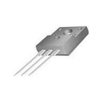
... FDP17N60N / FDPF17N60NT N-Channel MOSFET 600V, 17A, 0.34Ω Features • 0.29Ω ( Typ.)@ V = 10V, I DS(on) GS • Low Gate Charge ( Typ. 48nC) • Low C ( Typ. 23pF) rss • Fast Switching • 100% Avalanche Tested • Improved dv/dt Capability • RoHS Compliant TO-220 ...

Page 2

... R = 25Ω, Starting ≤ 17A, di/dt ≤ 200A/µs, V ≤ Starting DSS 4. Pulse Test: Pulse width ≤ 300µs, Duty Cycle ≤ Essentially Independent of Operating Temperature Typical Characteristics FDP17N60N/FDPF17N60NT Rev. A Package Reel Size TO-220 - TO-220F - unless otherwise noted C Test Conditions I = 250µA, V ...

Page 3

... I , Drain Current [A] D Figure 5. Capacitance Characteristics 10000 1000 *Note: 100 1MHz C iss = shorted C oss = rss = 0 Drain-Source Voltage [V] DS FDP17N60N/FDPF17N60NT Rev. A Figure 2. Transfer Characteristics µ s Pulse Test Figure 4. Body Diode Forward Voltage = 10V V = 20V GS o *Note Figure 6. Gate Charge Characteristics C iss C oss ...

Page 4

... 150 Single Pulse 0. Drain-Source Voltage [ 0.5 0.2 0.1 0.05 0.1 0.02 0.01 0.01 Single pulse 0.003 -5 10 FDP17N60N/FDPF17N60NT Rev. A (Continued) Figure 8. On-Resistance Variation 3.0 2.5 2.0 1.5 1.0 *Notes: 0 250 µ 0.0 50 100 150 Figure 10. Maximum Drain Current 20 10 µ s 100 µ ...

Page 5

... FDP17N60N/FDPF17N60NT Rev. A Gate Charge Test Circuit & Waveform Resistive Switching Test Circuit & Waveforms Unclamped Inductive Switching Test Circuit & Waveforms 5 www.fairchildsemi.com ...

Page 6

... FDP17N60N/FDPF17N60NT Rev. A Peak Diode Recovery dv/dt Test Circuit & Waveforms + + • • • I • www.fairchildsemi.com ...

Page 7

... Mechanical Dimensions FDP17N60N/FDPF17N60NT Rev. A TO-220 7 www.fairchildsemi.com ...

Page 8

... Package Dimensions * Front/Back Side Isolation Voltage : 4000V FDP17N60N/FDPF17N60NT Rev. A TO-220F Potted 8 Dimensions in Millimeters www.fairchildsemi.com ...

Page 9

... Definition of Terms Datasheet Identification Product Status Advance Information Formative / In Design Preliminary First Production No Identification Needed Full Production Obsolete Not In Production FDP17N60N/FDPF17N60NT Rev. A F-PFS™ PowerTrench ® FRFET PowerXS™ SM Global Power Resource Programmable Active Droop™ ® Green FPS™ QFET Green FPS™ ...

Related keywords