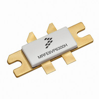
MRFE6VP6300HR5 Freescale Semiconductor, MRFE6VP6300HR5 Datasheet

MRFE6VP6300HR5
Specifications of MRFE6VP6300HR5
Available stocks
Related parts for MRFE6VP6300HR5
MRFE6VP6300HR5 Summary of contents
Page 1
... MTTF calculator available at http://www.freescale.com/rf. Select Software & Tools/Development Tools/Calculators to access MTTF calculators by product. 3. Refer to AN1955, Thermal Measurement Methodology of RF Power Amplifiers http://www.freescale.com/rf. Select Documentation/Application Notes -- AN1955. © Freescale Semiconductor, Inc., 2010. All rights reserved. RF Device Data Freescale Semiconductor = 100 mA ...
Page 2
... Vdc 1.7 2.5 3.2 Vdc — 0.25 — Vdc — 0.8 — pF — 76 — pF — 188 — 300 W Peak (60 W Avg.), f = 230 MHz, out 25.0 26.5 28.0 dB 72.0 74.0 — % — --16 -- Device Data Freescale Semiconductor ...
Page 3
... V Chip Capacitor C14, C15, C16 220 μF, 100 V Electolytic Capacitors C18, C19 18 pF Chip Capacitors L1 120 nH Inductor L2 17.5 nH Inductor R1 1000 Ω, 1/2 W Chip Resistor PCB 0.030″, ε Device Data Freescale Semiconductor + + L1 C9 C14 C15 DUT C3 Z9 Z10* ...
Page 4
... Figure 3. MRFE6VP6300HR3(HSR3) Test Circuit Component Layout MRFE6VP6300HR3 MRFE6VP6300HSR3 4 C14 C10 C17 MRFE6VP6300H/HS Rev. 2 C15 C13 C16 C12 C11 C18 C20 C19 RF Device Data Freescale Semiconductor ...
Page 5
... MHz Pulse Width = 100 μsec, 20% Duty Cycle 100 150 200 250 P , OUTPUT POWER (WATTS) PULSED out Figure 8. Pulsed Drain Efficiency versus Output Power RF Device Data Freescale Semiconductor TYPICAL CHARACTERISTICS — PULSED 60 C iss oss 57 P1dB = 55.4 dBm (344 rss 54 53 ...
Page 6
... TWO--TONE SPACING (MHz) Figure 11. Intermodulation Distortion Products versus Two- -Tone Spacing = 50 Vdc 230 MHz 230.1 MHz 900 mA 1100 mA 1400 mA 1600 mA 100 P , OUTPUT POWER (WATTS) PEP out Figure 13. Third Order Intermodulation Distortion versus Output Power RF Device Data Freescale Semiconductor 40 400 ...
Page 7
... Figure 14. MTTF versus Junction Temperature — Device Data Freescale Semiconductor TYPICAL CHARACTERISTICS 110 130 150 170 190 210 T , JUNCTION TEMPERATURE (°C) J This above graph displays calculated MTTF in hours when the device is operated Vdc 300 W Avg., and η DD out MTTF calculator available at http://www.freescale.com/rf. Select Software & ...
Page 8
... W Peak DD DQ out source load MHz Ω Ω 230 0.65 + j2.79 1.64 + j2. Test circuit impedance as measured from source gate to ground Test circuit impedance as measured from load drain to ground. Output Device Matching Under Network Test Z Z source load RF Device Data Freescale Semiconductor ...
Page 9
... RF Device Data Freescale Semiconductor PACKAGE DIMENSIONS MRFE6VP6300HR3 MRFE6VP6300HSR3 9 ...
Page 10
... MRFE6VP6300HR3 MRFE6VP6300HSR3 10 RF Device Data Freescale Semiconductor ...
Page 11
... RF Device Data Freescale Semiconductor MRFE6VP6300HR3 MRFE6VP6300HSR3 11 ...
Page 12
... MRFE6VP6300HR3 MRFE6VP6300HSR3 12 RF Device Data Freescale Semiconductor ...
Page 13
... For Software Part Number search at http://www.freescale.com, and select the “Part Number” link the Software & Tools tab on the part’s Product Summary page to download the respective tool. The following table summarizes revisions to this document. Revision Date 0 Oct. 2010 • Initial Release of Data Sheet RF Device Data Freescale Semiconductor REVISION HISTORY Description MRFE6VP6300HR3 MRFE6VP6300HSR3 13 ...
Page 14
... Freescale Semiconductor product could create a situation where personal injury or death may occur. Should Buyer ...


