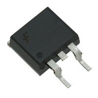
FJB3307DTM Fairchild Semiconductor, FJB3307DTM Datasheet
Home Discrete Semiconductor Products Transistors (BJT) - Single FJB3307DTM
Manufacturer Part Number
FJB3307DTM
Description
TRANS NPN FAST SW HV D2PAK
Manufacturer
Fairchild Semiconductor
Specifications of FJB3307DTM
Transistor Type
NPN
Current - Collector (ic) (max)
8A
Voltage - Collector Emitter Breakdown (max)
400V
Vce Saturation (max) @ Ib, Ic
3V @ 2A, 8A
Dc Current Gain (hfe) (min) @ Ic, Vce
5 @ 5A, 5V
Power - Max
1.72W
Mounting Type
Surface Mount
Package / Case
TO-263-3, D²Pak (2 leads + Tab), TO-263AB
Transistor Polarity
NPN
Mounting Style
SMD/SMT
Collector- Emitter Voltage Vceo Max
400 V
Emitter- Base Voltage Vebo
9 V
Collector- Base Voltage Vcbo
700 V
Maximum Dc Collector Current
16 A
Power Dissipation
1.72 W
Maximum Operating Temperature
+ 125 C
Continuous Collector Current
8 A
Dc Collector/base Gain Hfe Min
5
Minimum Operating Temperature
- 55 C
Lead Free Status / RoHS Status
Lead free / RoHS Compliant
Current - Collector Cutoff (max)
-
Frequency - Transition
-
Lead Free Status / Rohs Status
Lead free / RoHS Compliant
Other names
FJB3307DTMTR
Available stocks
© 2010 Fairchild Semiconductor Corporation
FJB3307D Rev. A0
FJB3307D
High Voltage Fast Switching NPN Power Transistor
Features
• Built-in Diode between Collector and Emitter
• Suitable for Electronic Ballast and Switch Mode Power Supplies
Absolute Maximum Ratings
* Pulse Test: PW = 300µs, Duty Cycle = 2% Pulsed
Thermal Characteristics
Symbol
Symbol
V
V
V
T
R
R
I
I
P
CBO
CEO
EBO
T
STG
I
CP
I
BP
C
B
θja
θjc
D
J
Collector-Base Voltage
Collector-Emitter Voltage
Emitter-Base Voltage
Collector Current (DC)
* Collector Current (Pulse)
Base Current (DC)
* Base Current (Pulse)
Junction Temperature
Storage Temperature
Total Device Dissipation
Thermal Resistance, Junction to Ambient
Thermal Resistance, Junction to Case
1.Base 2.Collector
1
Parameter
Parameter
D
T
2
a
-PAK
= 25°C unless otherwise noted
3.Emitter
T
T
a
c
= 25°C
= 25°C
1
B
Internal Schematic Diagram
-55 to 150
Value
Value
1.72
72.5
1.56
700
400
150
16
80
9
8
4
8
C
E
Units
Units
www.fairchildsemi.com
°C/W
°C/W
°C
°C
W
W
April 2010
V
V
V
A
A
A
A
Related parts for FJB3307DTM
FJB3307DTM Summary of contents
... Pulse Test 300µs, Duty Cycle = 2% Pulsed Thermal Characteristics Symbol P Total Device Dissipation D R Thermal Resistance, Junction to Ambient θja R Thermal Resistance, Junction to Case θjc © 2010 Fairchild Semiconductor Corporation FJB3307D Rev -PAK 3.Emitter T = 25°C unless otherwise noted a Parameter Parameter T = 25°C ...
... Output Capacitance ob t Storage Time STG t Fall Time F t Storage Time STG t Fall Time F * Pulse test 300µs, Duty Cycle = 2% Pulsed h Classification FE Classification h FE1 © 2010 Fairchild Semiconductor Corporation FJB3307D Rev 25°C unless otherwise noted a Conditions I = 500µ 5mA 500µ ...
... 0.1 0.01 0.01 0.1 I [A], COLLECTOR CURRENT C Figure 5. Collector Output Capacitance 1000 f = 1MHz 100 [V], COLLECTOR-BASE VOLTAGE CB © 2010 Fairchild Semiconductor Corporation FJB3307D Rev =300mA B I =250mA B I =200mA B I =150mA B I =100mA B I =50mA B 6.0 7.2 8.4 9.6 10.8 12.0 Figure 4 ...
... I [A], COLLECTOR CURRENT C Figure 11. Reverse Bias Safe Operating Area 200 300 400 V [V], COLLECTOR-EMITTER VOLTAGE CE © 2010 Fairchild Semiconductor Corporation FJB3307D Rev. A0 (Continued) Figure 8. Storage Time (Inductive Load) 3.00 2.75 2.50 2.25 2.00 1.75 1.50 1.25 1. 50V 1mH (off) = -5V -1.5V ...
... Mechanical Dimensions © 2010 Fairchild Semiconductor Corporation FJB3307D Rev -PAK 5 Dimensions in Millimeters www.fairchildsemi.com ...
... TRADEMARKS The following includes registered and unregistered trademarks and service marks, owned by Fairchild Semiconductor and/or its global subsidiaries, and is not intended exhaustive list of all such trademarks. AccuPower F-PFS Auto-SPM FRFET Build it Now Global Power Resource CorePLUS Green FPS CorePOWER Green FPS ...
Related keywords
FJB3307DTM datasheet FJB3307DTM data sheet FJB3307DTM pdf datasheet FJB3307DTM component FJB3307DTM part FJB3307DTM distributor FJB3307DTM RoHS FJB3307DTM datasheet download


