TCDT1102 Vishay, TCDT1102 Datasheet
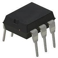
Transistor Output Optocouplers Phototransistor Out

TCDT1102

Manufacturer Part Number
TCDT1102
Description
Transistor Output Optocouplers Phototransistor Out
Manufacturer
Vishay
Datasheet

Specifications of TCDT1102

Isolation Voltage
3750 Vrms
Forward Current
60 mA
Maximum Input Diode Current
60 mA
Maximum Reverse Diode Voltage
5 V
Output Device
Transistor
Output Type
DC
Configuration
1
Input Type
DC
Maximum Collector Emitter Voltage
32 V
Maximum Collector Emitter Saturation Voltage
300 mV
Current Transfer Ratio
125 %
Maximum Forward Diode Voltage
1.6 V
Maximum Collector Current
50 mA
Maximum Power Dissipation
250 mW
Maximum Operating Temperature
+ 100 C
Minimum Operating Temperature
- 55 C
Package / Case
PDIP-6
No. Of Channels
1
Optocoupler Output Type
Phototransistor
Input Current
50mA
Output Voltage
32V
Opto Case Style
DIP
No. Of Pins
6
Input Current Max
50mA
Lead Free Status / RoHS Status
Lead free / RoHS Compliant
Lead Free Status / RoHS Status
Lead free / RoHS Compliant, Lead free / RoHS Compliant

Available stocks

Company
Part Number
Manufacturer
Quantity
Price
Part Number:
TCDT1102G
Manufacturer:
VISHAY/威世
Quantity:
20 000
TCDT1100/TCDT1100G
Vishay Semiconductors
DESCRIPTION
The
phototransistor optically coupled to a gallium arsenide
infrared-emitting diode in a 6-pin plastic dual inline package.
The base of the phototransistor is not connected providing
noise immunity.
The elements are mounted on one leadframe which
providing a fixed distance between input and output for
highest safety requirements.
VDE STANDARDS
These couplers perform safety functions according to the
following equipment standards:
• DIN EN 60747-5-5 pending
• IEC 60950/EN 60950
• VDE 0804
• IEC 60065
Note
G = leadform 10.16 mm; G is not marked on the body.
www.vishay.com
776
ORDER INFORMATION
PART
TCDT1100
TCDT1101
TCDT1102
TCDT1103
TCDT1100G
TCDT1101G
TCDT1102G
TCDT1103G
Optocoupler for electrical safety requirements
Office machines (applied for reinforced isolation for mains
voltage ≤ 400 V
Telecommunication apparatus and data processing
Safety
household apparatus
TCDT1100/TCDT1100G
A ( +)
for
NC
6
1
C (–)
C
2
5
mains-operated
RMS
NC
E
3
4
)
Optocoupler, Phototransistor Output
17201_1
For technical questions, contact: optocoupler.answers@vishay.com
series
D E
electronic
V
consists
and
related
of
a
FEATURES
• Isolation test voltage 5300 V
• Extra low coupling capacity - typical 0.2 pF
• High common mode rejection
• No base terminal connection for improved noise
• CTR offered in 4 groups
• Thickness though insulation ≥ 0.75 mm
• Creepage current resistance according to VDE 0303/
• Lead (Pb)-free component
• Component in accordance to RoHS 2002/95/EC and
APPLICATIONS
• Switch-mode power supplies
• Line receiver
• Computer peripheral interface
• Microprocessor system interface
• Circuits for safe protective separation against electrical
AGENCY APPROVALS
• UL1577, file no. E76222 system code A, double protection
• BSI IEC 60950; IEC 60065
• DIN EN 60747-5-5
• FIMKO
immunity
IEC 60112 comparative tracking index: CTI ≥ 275
WEEE 2002/96/EC
shock according to safety class II (reinforced isolation):
- for appl. class I - IV at mains voltage ≤ 300 V
- for appl. class I - III at mains voltage ≤ 600 V
according to DIN EN 60747-5-5.
CTR 100 to 200 %, DIP-6
CTR 63 to 125 %, DIP-6
CTR 40 to 80 %, DIP-6
CTR > 40 %, DIP-6
CTR > 40 %, DIP-6
REMARKS
RMS
Document Number: 83535
Rev. 1.6, 16-May-08

Related parts for TCDT1102

TCDT1102 Summary of contents

Page 1

... ORDER INFORMATION PART TCDT1100 TCDT1101 TCDT1102 TCDT1103 TCDT1100G TCDT1101G TCDT1102G TCDT1103G Note G = leadform 10.16 mm not marked on the body. www.vishay.com For technical questions, contact: optocoupler.answers@vishay.com 776 FEATURES • Isolation test voltage 5300 V • Extra low coupling capacity - typical 0.2 pF • ...

Page 2

... Minimum and maximum values are testing requierements. Typical values are characteristics of the device and are the result of engineering evaluations. Typical values are for information only and are not part of the testing requirements. Document Number: 83535 For technical questions, contact: optocoupler.answers@vishay.com Rev. 1.6, 16-May-08 (1) TEST CONDITION ≤ ...

Page 3

... T - Safety Temperature (°C) 94 9182 si Fig Derating Diagram www.vishay.com For technical questions, contact: optocoupler.answers@vishay.com 778 Optocoupler, Phototransistor Output PART SYMBOL TCDT1100 TCDT1100G TCDT1101 TCDT1101G = TCDT1102 TCDT1102G TCDT1103 TCDT1103G TEST CONDITION SYMBOL diss V IOTM T si TEST CONDITION SYMBOL 100 %, test IOTM Tr test ...

Page 4

... 0. µs p Channel I Channel II 50 Ω 1 kΩ 95 10843 Fig Test Circuit, Saturated Operation Document Number: 83535 For technical questions, contact: optocoupler.answers@vishay.com Rev. 1.6, 16-May-08 TEST CONDITION SYMBOL = 100 Ω, (see figure mA 100 Ω, (see figure mA 100 Ω, (see figure mA 100 Ω, (see figure 3) ...

Page 5

... T - Ambient Temperature (°C) amb Fig Relative Current Transfer Ratio vs. Ambient Temperature www.vishay.com For technical questions, contact: optocoupler.answers@vishay.com 780 Optocoupler, Phototransistor Output 10 000 80 120 95 11026 Fig Collector Dark Current vs. Ambient Temperature 1.4 1.6 1.8 2.0 95 11054 Fig ...

Page 6

... Fig Turn-on/off Time vs. Forward Current 20 Non-saturated t operation off Collector Current (mA) 95 11016 C Fig Turn-on/off Time vs. Collector Current Document Number: 83535 For technical questions, contact: optocoupler.answers@vishay.com Rev. 1.6, 16-May-08 Customer code/ identification/ option 100 10 Vishay logo 17936 t off 100 Ω TCDT1100/TCDT1100G Vishay Semiconductors XXXXX ...

Page 7

... TCDT1100/TCDT1100G Vishay Semiconductors PACKAGE DIMENSIONS in millimeters 0.3 A 0.58 max. A 0.3 A 0.58 max. A www.vishay.com For technical questions, contact: optocoupler.answers@vishay.com 782 Optocoupler, Phototransistor Output 8.8 max. 8.6 max. 1.54 2.54 nom. 5.08 nom. Weight: ca. 0. Creepage distance: > Air path: > after mounting on PC board ...

Page 8

... The Montreal Protocol (1987) and its London Amendments (1990) intend to severely restrict the use of ODSs and forbid their use within the next ten years. Various national and international initiatives are pressing for an earlier ban on these substances. Vishay Semiconductor GmbH has been able to use its policy of continuous improvements to eliminate the use of ODSs listed in the following documents. ...

Page 9

... Vishay disclaims any and all liability arising out of the use or application of any product described herein or of any information provided herein to the maximum extent permitted by law. The product specifications do not expand or otherwise modify Vishay’ ...

Related keywords