V2DIP1-48 FTDI, V2DIP1-48 Datasheet - Page 3
V2DIP1-48
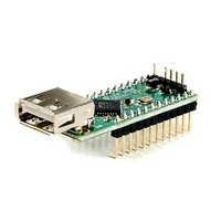
Manufacturer Part Number
V2DIP1-48
Description
Interface Modules & Development Tools USB Vinculum-II 48 Pin Mod 1 USB Port
Manufacturer
FTDI
Datasheet
1.V2DIP1-48.pdf
(25 pages)
Specifications of V2DIP1-48
Interface Type
USB, Serial, UART, FIFO, SPI
Data Bus Width
Serial, 8 bit
Operating Supply Voltage
5 V
Product
Interface Modules
For Use With/related Products
VNC2-48
Lead Free Status / RoHS Status
Lead free / RoHS Compliant


1
2
3
4
5
6
7
8
3.1
3.2
3.3
3.4
3.5
3.6
3.7
3.8
3.9
4.1
4.2
4.3
5.1
Appendix A – References ............................................................................................ 22
Appendix B – List of Figures and Tables ................................................................... 23
List of Figures............................................................................................................... 23
List of Tables ................................................................................................................ 23
Appendix C – Revision History ................................................................................... 24
Introduction............................................................................................ 1
Features ................................................................................................. 3
Pin Out and Signal Description ............................................................ 4
3.5.1
3.6.1
3.6.2
3.7.1
3.7.2
3.8.1
3.9.1
Firmware .............................................................................................. 17
External circuit Configuration ............................................................ 18
Mechanical Dimensions ...................................................................... 19
Schematic Diagram ............................................................................. 20
Contact Information............................................................................. 21
Module Pin Out .................................................................................................... 4
Pin Signal Description ........................................................................................ 6
I/O Configuration Using The Jumper Pin Header ............................................. 8
Default Interface I/O Pin Configuration .............................................................. 9
UART Interface ................................................................................................... 10
Serial Peripheral Interface (SPI) ....................................................................... 11
Parallel FIFO Interface-Asynchronous Mode .................................................. 12
Parallel FIFO Interface-Synchronous Mode .................................................... 14
Debugger Interface ............................................................................................ 16
Firmware Support .............................................................................................. 17
Available Firmware ............................................................................................ 17
Firmware Upgrades ........................................................................................... 17
Adding a second USB Port ............................................................................... 18
Signal Description – UART Interface .............................................................................. 10
Signal Description - SPI Slave ........................................................................................ 11
Signal Description - SPI Master ...................................................................................... 11
Signal Description - Parallel FIFO Interface ................................................................. 12
Timing Diagram – Asynchronous FIFO Mode Read and Write Cycle ..................... 13
Timing Diagram – Synchronous FIFO Mode Read and Write Cycle ....................... 14
Signal Description - Debugger Interface ...................................................................... 16
Copyright © 2010 Future Technology Devices International Limited
`
Table of Contents
V2DIP1-48 VNC2-48 Development Module Datasheet Version 1.0
Document Reference No.: FT_000236
Clearance No.: FTDI# 153
2
Related parts for V2DIP1-48
Image
Part Number
Description
Manufacturer
Datasheet
Request
R

Part Number:
Description:
MOD MCU-USB HOST CTLR 24-DIP
Manufacturer:
FTDI, Future Technology Devices International Ltd
Datasheet:

Part Number:
Description:
MOD MCU-USB HOST CTLR 60-DIP
Manufacturer:
FTDI, Future Technology Devices International Ltd
Datasheet:

Part Number:
Description:
BOARD, EVALUATION, UK PSU
Manufacturer:
FTDI
Datasheet:
Part Number:
Description:
BOARD, EVALUATION, US PSU
Manufacturer:
FTDI
Datasheet:
Part Number:
Description:
Specifications: Manufacturer: FTDI ; Product Category: USB Interface IC ; RoHS: Details ; Operating Supply Voltage: 3 V to 5.25 V ; Supply Current: 25 mA ; Maximum Operating Temperature: + 70 C ; Mounting Style: SMD/SMT ; Package / Case: QFN-32
Manufacturer:
FTDI
Part Number:
Description:
integr. usb2.0/uart lqfp32 rohs ftdi reel c1k...
Manufacturer:
FTDI
Datasheet:
Part Number:
Description:
Interface Development Tools USB to UART Breakout Board
Manufacturer:
FTDI
Datasheet:

Part Number:
Description:
IC USB TO SERIAL UART 32-QFN
Manufacturer:
FTDI, Future Technology Devices International Ltd

Part Number:
Description:
USB Interface IC USB to Serial UART Enhanced IC SSOP-28
Manufacturer:
FTDI
Datasheet:

Part Number:
Description:
IC, USB UART INTERFACE, SSOP-28
Manufacturer:
FTDI
Datasheet:

Part Number:
Description:
IC, USB UART INTERFACE, QFN-32
Manufacturer:
FTDI
Datasheet:
Part Number:
Description:
IC, USB FIFO INTERFACE, SSOP-28
Manufacturer:
FTDI
Datasheet:
Part Number:
Description:
MODULE, USB, 4 PORT, FT4232H BASED
Manufacturer:
FTDI
Datasheet:
Part Number:
Description:
357-036-542-201 CARDEDGE 36POS DL .156 BLK LOPRO
Manufacturer:
FTDI
Datasheet:
Part Number:
Description:
357-036-542-201 CARDEDGE 36POS DL .156 BLK LOPRO
Manufacturer:
FTDI
Datasheet: