VNCLO-SHLD-1A FTDI, VNCLO-SHLD-1A Datasheet
VNCLO-SHLD-1A
Specifications of VNCLO-SHLD-1A


Related parts for VNCLO-SHLD-1A


VNCLO-SHLD-1A Summary of contents
Page 1
... Unit 1, 2 Seaward Place, Centurion Business Park, Glasgow, G41 1HH, United Kingdom Tel.: +44 (0) 141 429 2777 Use of FTDI devices in life support and/or safety applications is entirely at the user’s risk, and the user agrees to defend, indemnify and hold harmless FTDI from any and all damages, claims, suits or expense resulting from such use. Copyright © ...
Page 2
... Introduction Vinco is a development module based on the FTDI Vinculum II, VNC2 dual USB host/slave IC. Vinco is designed as a prototyping platform for VNC2 based designs and applications. The mechanical form of the module, and the concept of providing free software development library and tools, is inspired by the Arduino concept. Vinco is a superset of the Duemilanove / Uno with 2 extra rows of headers providing an extra 10 pins. The Vinco programming language utilises a subset of standard ANSII ‘ ...
Page 3
... Interface Devices (keyboards, mice), audio devices, video devices (webcam) with many more under development. Precompiled driver support for a wide range of USB device classes including FTDI peripheral ICs, Human Interface Devices (keyboards, mice) with many more under developed. Compatible with existing Arduino shields. ...
Page 4
... Vinco Motherboard Vinco +9V/1A PSU ( Optional ) - USA Vinco +9V/1A PSU ( Optional ) - Europe Vinco +9V/1A PSU ( Optional ) - UK Vinco_Proto prototyping shield (Optional) VNC2 debugger/programmer module Vinco and a debugger/programmer module VNCLO-START1 VNCLO-SHLD-1A * 2pc VNCLO-PSU-XX (dependent regional requirement (UK/US/EU) A mini B cable USB A to mini-"B" Cable ...
Page 5
... Firmware Support ................................................................... 14 7.2 Available Firmware ................................................................. 14 7.3 Firmware Upgrades ................................................................. 14 7.4 Arduino Shield Compatible Firmware ...................................... 14 8 Mechanical Dimensions ................................................. 15 9 Schematic Diagram ....................................................... 16 Copyright © 2010-2011 Future Technology Devices International Limited Document Reference No.: FT_000327 Vinco Development Module Datasheet Version 2.0 Table of Contents Clearance No.: FTDI#173 1 ...
Page 6
... Arduino Shields ............................................................. 17 11 Contact Information ...................................................... 18 Appendix A – References ................................................................. 20 Appendix B – List of Figures and Tables .......................................... 21 List of Figures ................................................................................. 21 List of Tables ................................................................................... 21 Appendix C – Revision History ......................................................... 22 Copyright © 2010-2011 Future Technology Devices International Limited Document Reference No.: FT_000327 Vinco Development Module Datasheet Version 2.0 Clearance No.: FTDI#173 2 ...
Page 7
... PWREN signal that controls the power output to the USB Host connector, CN2. PWREN# is connected to the VNC2-64Q IC on pin 41. Configure this pin for a GPIO output in order to make power available at CN2 for USB peripherals. Copyright © 2010-2011 Future Technology Devices International Limited Document Reference No.: FT_000327 Vinco Development Module Datasheet Version 2.0 Clearance No.: FTDI#173 3 ...
Page 8
... Vinco Development Module Datasheet Version 2.0 CN2 CN1 LED3 JP1 SW2 1 JP2 Interface to shield boards Interface to shield boards Interface to shield boards Interface to shield boards Interface to shield boards Interface to shield boards Clearance No.: FTDI#173 FUNCTION Power input USB host port USB slave port Debug port 4 ...
Page 9
... I/O 5V safe bidirectional data / control bus bit 37 I/O 5V safe bidirectional data / control bus bit 38 I/O 5V safe bidirectional data / control bus bit 39 I/O 5V safe bidirectional data / control bus bit 6 I/O 5V safe bidirectional data / control bus bit 7 Clearance No.: FTDI#173 Description 5 ...
Page 10
... Not connected – used as a key for VII Debugger NV module GND GND for PCB Input Reset for the VNC2-64Q Used to put the VNC2-64Q into PROGRAM mode if Input loading ROM file over UART PWR Input May be used by debugger to power module Clearance No.: FTDI#173 6 ...
Page 11
... The port is USB 2.0 full speed compliant. Pin No. Signal 5V supply to peripheral 1 device. Enabled by the VNC2-64Q 2 USB DM 3 USB DP 4 GND Table 3.4 – USB Slave Pin Out Copyright © 2010-2011 Future Technology Devices International Limited Document Reference No.: FT_000327 Vinco Development Module Datasheet Version 2.0 Clearance No.: FTDI#173 7 ...
Page 12
... Copyright © 2010-2011 Future Technology Devices International Limited Document Reference No.: FT_000327 Vinco Development Module Datasheet Version 2.0 Connect pins 1-2 Vinco is Powered from USB host via CN3 ADC reference voltage = 3V3 Clearance No.: FTDI#173 Connect Pins 2-3 Vinco is Powered from external 9V supply ADC reference voltage = 5V0 8 ...
Page 13
... TXDEN transmit operation is in progress. The uart_tx_active Output TXDEN signal will be set high one bit-time before data is transmitted and return low one bit time after the last bit of a data frame has been transmitted Clearance No.: FTDI#173 Description may be used to signal that a 9 ...
Page 14
... Output spi_m_mosi Output spi_m_miso Input spi_m_ss_0# Output spi_m_ss_1# Output Clearance No.: FTDI#173 Description Slave clock input Master Out Slave In Synchronous data from master to slave Master In Slave Out Synchronous data from slave to master Slave chip select Description SPI master clock input (J4-6 is the default) ...
Page 15
... Parallel FIFO Interface - Asynchronous Mode The Parallel FIFO Asynchronous mode is functionally the same as the Parallel FIFO Interface available in the FTDI VDIP1 module and has an eight bit data bus, individual read and write strobes and two hardware flow control signals. 4.3.1 Signal Description - Parallel FIFO Interface The Parallel FIFO Interface signals can be programmed to a choice of available I/O pins ...
Page 16
... VNC2. 5.0V module supply pin. This pin can be used to provide the 5.0V input to the Vinco from the PWR Input debugger interface when the Vinco is not powered from the USB connector (VBUs) or the CN1 Document Reference No.: FT_000327 Clearance No.: FTDI#173 Description 12 ...
Page 17
... MCP3008 analogue input channel 2 / Input VNC2-64Q PWM2 MCP3008 analogue input channel 3 / Input VNC2-64Q PWM3 MCP3008 analogue input channel 4 / Input VNC2-64Q PWM4 MCP3008 analogue input channel 5 / Input VNC2-64Q PWM5 MCP3008 analogue input channel 6 / Input VNC2-64Q PWM6 MCP3008 analogue input channel 7 / Input VNC2-64Q PWM7 Clearance No.: FTDI#173 13 ...
Page 18
... Additionally with the IDE it will be possible for users to develop new shields and applications. Copyright © 2010-2011 Future Technology Devices International Limited Document Reference No.: FT_000327 Vinco Development Module Datasheet Version 2.0 FTDI website. However the VNC2-64Q on the Vinco can be for full details on available pre-compiled firmware. Clearance No.: FTDI#173 14 ...
Page 19
... Figure 8.1 – Vinco Dimensions – Figure 8.2 Vinco Pitch Measurements ±0.20mm Tolerance (except pitch) Maximum height is 15mm All dimensions are in mm Copyright © 2010-2011 Future Technology Devices International Limited Document Reference No.: FT_000327 Vinco Development Module Datasheet Version 2.0 Clearance No.: FTDI#173 15 ...
Page 20
... Schematic Diagram Figure 9.1 – Vinco Schematics Copyright © 2010-2011 Future Technology Devices International Limited Document Reference No.: FT_000327 Vinco Development Module Datasheet Version 2.0 Clearance No.: FTDI#173 16 ...
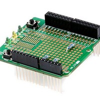
Page 21
... This shield includes connectors and an assortment of resistors and LEDs to provide a starting point aimed at the hobbyist. Figure 10.1 – Vinco_Proto Copyright © 2010-2011 Future Technology Devices International Limited Document Reference No.: FT_000327 Vinco Development Module Datasheet Version 2.0 Clearance No.: FTDI#173 17 ...
Page 22
... E-Mail (General Enquiries): Web Site URL Distributor and Sales Representatives Please visit the Sales Network page of the FTDI Web site for the contact details of our distributor(s) and sales representative(s) in your country. Copyright © 2010-2011 Future Technology Devices International Limited Vinco Development Module Datasheet Version 2.0 sales1@ftdichip ...
Page 23
... FTDI. Use of FTDI devices in life support and/or safety applications is entirely at the user’s risk, and the user agrees to defend, indemnify and hold harmless FTDI from any and all damages, claims, suits or expense resulting from such use. This document is subject to change without notice ...
Page 24
... Migrating Vinculum Designs From VNC1L to VNC2-48L1A Vinculum-II Toolchain Installation Guide Vinculum-II Toolchain Getting Started Guide Vinculum-II User Guide MCP3008 Datasheet (http://ww1.microchip.com/downloads/en/DeviceDoc/21295d.pdf) Copyright © 2010-2011 Future Technology Devices International Limited Document Reference No.: FT_000327 Vinco Development Module Datasheet Version 2.0 http://www.ftdichip.com/Support/Documents/AppNotes.htm Clearance No.: FTDI#173 20 ...
Page 25
... Table 4.4 – Data and Control Bus Signal Mode Options – Parallel FIFO Interface ................................. 11 Table 5.1 – Signal Name and Description – Debugger Interface ........................................................ 12 Table 6.1 – ADC Interface ............................................................................................................ 13 Copyright © 2010-2011 Future Technology Devices International Limited Document Reference No.: FT_000327 Vinco Development Module Datasheet Version 2.0 Clearance No.: FTDI#173 21 ...
Page 26
... Vinculo module Updated the disclaimer. Renamed the debugger module to VNC2 debugger/programming module. Section 1: Added text about debugger/programmer module Section 1.3: Added part number VNCLO-START1 Updated table 3.1(Description), 4.1, 4.2, 4.3 and 4.4 (Available pins) Version 1.4 Added part number Version 1.5 ...