NJM4560M-TE1 NJR, NJM4560M-TE1 Datasheet

Op Amps Dual High Gain

NJM4560M-TE1

Manufacturer Part Number
NJM4560M-TE1
Description
Op Amps Dual High Gain
Manufacturer
NJR
Datasheet

Specifications of NJM4560M-TE1

Number Of Channels
2
Common Mode Rejection Ratio (min)
70 dB
Input Offset Voltage
6 mV
Input Bias Current (max)
500 nA
Supply Current
5.7 mA
Maximum Power Dissipation
300 mW
Maximum Operating Temperature
+ 85 C
Minimum Operating Temperature
- 40 C
Dual Supply Voltage
+/- 5 V, +/- 9 V, +/- 12 V, +/- 15 V
Maximum Dual Supply Voltage
+/- 18 V
Minimum Dual Supply Voltage
+/- 4 V
Mounting Style
SMD/SMT
Shutdown
No
Technology
Bipolar
Voltage Gain Db
100 dB
Slew Rate
4 V/us
Package / Case
DMP-8
Lead Free Status / RoHS Status
Lead free / RoHS Compliant
■ GENERAL DESCRIPTION
bandwidth, dual operational amplifier capable of driving 20V
peak-to-peak into 400Ω loads. The NJM4560 combines
many of the features of the NJM4558 as well as providing the
capability of wider bandwidth, and higher slew rate make the
NJM4560 ideal for active filters, data and telecommunications,
and many instrumentation applications. The availability of the
NJM4560 in the surface mounted micro-package allows the
NJM4560 to be used in critical applications requiring very high
packing densities.
■ FEATURES
■ PIN CONFIGURATION
■ EQUIVALENT CIRCUIT ( 1/2 Shown )
Ver.2006-11-17
● Operating Voltage
● Wide Gain Bandwidth Product
● Slew Rate
● Package Outline
● Bipolar Technology
The NJM4560 integrated circuit is a high-gain, wide
NJM4560D/M/E
DUAL OPERATIONAL AMPLIFIER
( ±4V~±18V )
( 10MHz typ. )
( 4V/µs typ. )
DIP8, DMP8, EMP8, SIP8
NJM4560L
PIN FUNCTION
1.A OUTPUT
2.A –INPUT
3.A +INPUT
4.V
5.B +INPUT
6.B –INPUT
7.B OUTPUT
8.V
-
+
■ PACKAGE OUTLINE
NJM4560D
NJM4560E
NJM4560M
NJM4560L
- 1 -

Related parts for NJM4560M-TE1

NJM4560M-TE1 Summary of contents

Page 1

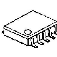
... NJM4560D/M/E ■ EQUIVALENT CIRCUIT ( 1/2 Shown ) Ver.2006-11-17 ( ±4V~±18V ) ( 10MHz typ 4V/µs typ. ) DIP8, DMP8, EMP8, SIP8 PIN FUNCTION 1.A OUTPUT 2.A –INPUT 3.A +INPUT - 4.V 5.B +INPUT 6.B –INPUT NJM4560L 7.B OUTPUT + 8.V ■ PACKAGE OUTLINE NJM4560M NJM4560D NJM4560E NJM4560L - 1 - ...

Page 2

ABSOLUTE MAXIMUM RATINGS PARAMETER Supply Voltage Differential Input Voltage Input Voltage Power Dissipation Operating Temperature Range Storage Temperature Range ( note ) For supply voltage less than ±15V,the absolute maximum input voltage is equal to the supply voltage. ■ ...

Page 3

TYPICAL CHARACTERISTICS Ver.2006-11- ...

Page 4

TYPICAL CHARACTERISTICS - 4 - [CAUTION] The specifications on this databook are only given for information , without any guarantee as regards either mistakes or omissions. The application circuits in this databook are described only to show representative usages ...

Related keywords