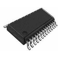
WM8510GEDS/V Wolfson Microelectronics, WM8510GEDS/V Datasheet - Page 61

WM8510GEDS/V
Manufacturer Part Number
WM8510GEDS/V
Description
Audio CODECs VoIP Mono CODEC
Manufacturer
Wolfson Microelectronics
Datasheet
1.WM8510GEDSV.pdf
(82 pages)
Specifications of WM8510GEDS/V
Operating Supply Voltage
- 0.3 V to + 7 V
Maximum Operating Temperature
+ 85 C
Mounting Style
SMD/SMT
Package / Case
SSOP-28
Minimum Operating Temperature
- 25 C
Lead Free Status / RoHS Status
Lead free / RoHS Compliant
Production Data
POWER MANAGEMENT
w
Table 52 Typical POR Operation (typical values, not tested)
Notes:
1.
2.
3.
4.
5.
The VMIDSEL and BIASEN bits must be set to enable analogue output midrail voltage and for
normal DAC operation.
SAVING POWER BY REDUCING OVERSAMPLING RATE
The default mode of operation of the ADC and DAC digital filters is in 64x oversampling mode. Under
the control of ADCOSR and DACOSR the oversampling rate may be doubled. 64x oversampling
results in a slight decrease in noise performance compared to 128x but lowers the power
consumption of the device.
Table 53 ADC and DAC Oversampling Rate Selection
R10
DAC control
R14
ADC control
t
t
t
t
hp__midrail_off
line_midrail_on
line_midrail_off
hp_midrail_on
SYMBOL
The lineout charge time, t
time is dependent upon the value of VMID decoupling capacitor and VMID pin input resistance
and AVDD power supply rise time. The values above were measured using a 4.7 µ F capacitor.
It is not advisable to allow DACDAT data input during initialisation of the DAC. If the DAC data
value is not zero at point of initialisation, then this is likely to cause a pop noise on the analogue
outputs. The same is also true if the DACDAT is removed at a non-zero value, and no mute
function has been applied to the signal beforehand.
The lineout discharge time, t
capacitor and the leakage resistance path to ground. The values above were measured using a
10 µ F output capacitor.
The headphone charge time, t
capacitor and VMID pin input resistance and AVDD power supply rise time. The values above
were measured using a 4.7 µ F VMID decoupling capacitor.
The headphone discharge time, t
coupling capacitor and the leakage resistance path to ground. The values above were
measured using a 100 µ F capacitor.
REGISTER
ADDRESS
t
dacint
MIN
3
3
BIT
TYPICAL
line_midrail_on,
500
500
2/fs
1
6
line_midrail_off,
DACOSR128
ADCOSR128
hp_midrail_on,
LABEL
hp_midrail_off,
MAX
is mainly determined by the VMID pin charge time. This
is dependent upon the value of the lineout coupling
is dependent upon the value of VMID decoupling
is dependent upon the value of the headphone
UNIT
n /fs
0
0
ms
ms
s
s
DEFAULT
DAC oversample rate select
0 = 64x (lowest power)
1 = 128x (best SNR)
ADC oversample rate select
0 = 64x (lowest power)
1 = 128x (best SNR)
PD, Rev 4.5, September 2008
DESCRIPTION
WM8510
61


