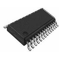
WM8510GEDS/V Wolfson Microelectronics, WM8510GEDS/V Datasheet - Page 73

WM8510GEDS/V
Manufacturer Part Number
WM8510GEDS/V
Description
Audio CODECs VoIP Mono CODEC
Manufacturer
Wolfson Microelectronics
Datasheet
1.WM8510GEDSV.pdf
(82 pages)
Specifications of WM8510GEDS/V
Operating Supply Voltage
- 0.3 V to + 7 V
Maximum Operating Temperature
+ 85 C
Mounting Style
SMD/SMT
Package / Case
SSOP-28
Minimum Operating Temperature
- 25 C
Lead Free Status / RoHS Status
Lead free / RoHS Compliant
Production Data
w
REGISTER
44 (2Ch)
45 (2Dh)
47 (2Fh)
ADDRESS
8
7:4
3
2
1
0
8
7
6
5:0
8
7
6:4
3
BIT
MBVSEL
MIC2MODE
MIC2_2INPP
GA
MICN2INPPGA
MICP2INPPGA
INPPGAZC
INPPGAMUTE
INPPGAVOL
PGABOOST
MICP2BOOST
VOL
LABEL
0
0
0000
0
1
1
0
0
0
010000
1
0
000
0
DEFAULT
Microphone Bias Voltage Control
0 = 0.9 * AVDD
1 = 0.75 * AVDD
Reserved
Auxiliary Input Mode
0 = inverting buffer
1 = mixer (on-chip input resistor bypassed)
Select AUX amplifier output as input PGA signal
source.
0=AUX not connected to input PGA
1=AUX connected to input PGA amplifier negative
terminal.
Connect MICN to input PGA negative terminal.
0=MICN not connected to input PGA
1=MICN connected to input PGA amplifier negative
terminal.
Connect input PGA amplifier positive terminal to MICP
or VMID.
0 = input PGA amplifier positive terminal connected to
VMID
1 = input PGA amplifier positive terminal connected to
MICP through variable resistor string
Reserved
Input PGA zero cross enable:
0=Update gain when gain register changes
1=Update gain on 1
write.
Mute control for input PGA:
0=Input PGA not muted, normal operation
1=Input PGA muted (and disconnected from the
following input BOOST stage).
Input PGA volume
000000 = -12dB
000001 = -11.25db
.
010000 = 0dB
.
111111 = 35.25dB
Input Boost
0 = PGA output has +0dB gain through input BOOST
stage.
1 = PGA output has +20dB gain through input BOOST
stage.
Reserved
Controls the MICP pin to the input boost stage (NB,
when using this path set MICP2INPPGA=0):
000=Path disabled (disconnected)
001=-12dB gain through boost stage
010=-9dB gain through boost stage
…
111=+6dB gain through boost stage
Reserved
DESCRIPTION
st
zero cross after gain register
PD, Rev 4.5, September 2008
Input Signal
Path
Input Signal
Path
Input Signal
Path
Input Signal
Path
Input Signal
Path
Input Signal
Path
Input Signal
Path
Input Signal
Path
Input Signal
Path
Input Signal
Path
REFER TO
WM8510
73


