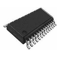
WM8510GEDS/RV Wolfson Microelectronics, WM8510GEDS/RV Datasheet - Page 42

WM8510GEDS/RV
Manufacturer Part Number
WM8510GEDS/RV
Description
Audio CODECs VolP MONO CODEC 28-pin
Manufacturer
Wolfson Microelectronics
Datasheet
1.WM8510GEDSV.pdf
(82 pages)
Specifications of WM8510GEDS/RV
Operating Supply Voltage
- 0.3 V to + 7 V
Maximum Operating Temperature
+ 85 C
Mounting Style
SMD/SMT
Package / Case
SSOP-28
Minimum Operating Temperature
- 25 C
Lead Free Status / RoHS Status
Lead free / RoHS Compliant
Available stocks
Company
Part Number
Manufacturer
Quantity
Price
Part Number:
WM8510GEDS/RV
Manufacturer:
WOLFSON
Quantity:
20 000
WM8510
w
Table 29 Output Boost Control
Table 30 Output Boost Stage Details
SPKOUTP/SPKOUTN OUTPUTS
The SPKOUT pins can drive a single bridge tied 8 Ω speaker or two headphone loads of 16Ω or 32Ω
or a line output (see Headphone Output and Line Output sections, respectively). The signal to be
output on SKPKOUT comes from the Speaker Mixer circuit and can be any combination of the DAC
output, the Bypass path (output of the boost stage) and the MIC2 input.
option of 0dB or -10dB attenuation, selected by the SPKATTN register bit. The SPKOUTP/N volume
is controlled by the SPKVOL register bits. Note that gains over 0dB may cause clipping if the signal
is large. The SPKMUTE register bit causes the speaker outputs to be muted (the output DC level is
driven out). The output pins remains at the same DC level (VMIDOP), so that no click noise is
produced when muting or un-muting.
The SPKOUTN pin always drives out an inverted version of the SPKOUTP signal.
Table 31 Speaker Mixer Control
R49
Output control
R1
Power
management 1
R50
Speaker mixer
control
R40
Bypass path
attenuation
control
MONOBOOST
SPKBOOST/
REGISTER
REGISTER
ADDRESS
ADDRESS
0
1
2
3
8
0
1
5
1
BIT
BIT
STAGE GAIN
OUTPUT
1.5x
1x
SPKBOOST
BUFDCOPEN
DAC2SPK
BYP2SPK
MIC2_2SPK
SPKATTN
MONOBOOST
LABEL
LABEL
OUTPUT DC
1.5xAVDD/2
AVDD/2
LEVEL
DEFAULT
0
0
0
DEFAULT
1
0
0
0
Speaker output boost stage control
(see Table 30 for details)
0=No boost (outputs are inverting
buffers)
1 = 1.5x gain boost
Mono output boost stage control (see
Table 30 for details)
0=No boost (output is inverting buffer)
1=1.5x gain boost
Dedicated buffer for DC level shifting
output stages when in 1.5x gain boost
configuration.
0=Buffer disabled
1=Buffer enabled (required for 1.5x
gain boost)
CONFIGURATION
OUTPUT STAGE
Output of DAC to speaker mixer input
0 = not selected
1 = selected
Bypass path (output of input boost
stage) to speaker mixer input
0 = not selected
1 = selected
Output of MIC2 amplifier to speaker
mixer input
0 = not selected
1 = selected
Attenuation control for bypass path
(output of input boost stage) to
speaker mixer input
0 = 0dB
1 = -10dB
Non-inverting
Inverting
PD, Rev 4.5 ,September 2008
DESCRIPTION
DESCRIPTION
The Bypass path has the
Production Data
42


