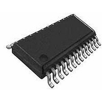
WM8510GEDS/RV Wolfson Microelectronics, WM8510GEDS/RV Datasheet - Page 56

WM8510GEDS/RV
Manufacturer Part Number
WM8510GEDS/RV
Description
Audio CODECs VolP MONO CODEC 28-pin
Manufacturer
Wolfson Microelectronics
Datasheet
1.WM8510GEDSV.pdf
(82 pages)
Specifications of WM8510GEDS/RV
Operating Supply Voltage
- 0.3 V to + 7 V
Maximum Operating Temperature
+ 85 C
Mounting Style
SMD/SMT
Package / Case
SSOP-28
Minimum Operating Temperature
- 25 C
Lead Free Status / RoHS Status
Lead free / RoHS Compliant
Available stocks
Company
Part Number
Manufacturer
Quantity
Price
Part Number:
WM8510GEDS/RV
Manufacturer:
WOLFSON
Quantity:
20 000
WM8510
GENERAL PURPOSE INPUT/OUTPUT
CONTROL INTERFACE
w
The CSB/GPIO pin can be configured to perform a variety of useful tasks by setting the GPIOSEL
register bits. The GPIO is only available in 2 wire mode.
Note that SLOWCLKEN must be enabled when using the Jack Detect function
Table 49 CSB/GPIO Control
SELECTION OF CONTROL MODE AND 2-WIRE MODE ADDRESS
The control interface can operate as either a 3-wire or 2-wire MPU interface. The MODE pin
determines the 2 or 3 wire mode as shown in Table 50.
The WM8510 is controlled by writing to registers through a serial control interface. A control word
consists of 16 bits. The first 7 bits (B15 to B9) are address bits that select which control register is
accessed. The remaining 9 bits (B8 to B0) are register bits, corresponding to the 9 bits in each
control register.
Table 50 Control Interface Mode Selection
3-WIRE SERIAL CONTROL MODE
In 3-wire mode, every rising edge of SCLK clocks in one data bit from the SDIN pin. A rising edge on
CSB/GPIO latches in a complete control word consisting of the last 16 bits.
R8
GPIO
control
REGISTER
ADDRESS
MODE
High
Low
2:0
3
5:4
BIT
GPIOSEL
GPIOPOL
OPCLKDIV
LABEL
INTERFACE FORMAT
2 wire
3 wire
000
0
00
DEFAULT
CSB/GPIO pin function select:
000=CSB input
001= Jack insert detect
010=Temp ok
011=Amute active
100=PLL clk o/p
101=PLL lock
110=Reserved
111=Reserved
GPIO Polarity invert
0=Non inverted
1=Inverted
PLL Output clock division ratio
00=divide by 1
01=divide by 2
10=divide by 3
11=divide by 4
PD, Rev 4.5 ,September 2008
DESCRIPTION
Production Data
56


