WM8510GEDS/RV Wolfson Microelectronics, WM8510GEDS/RV Datasheet - Page 58
WM8510GEDS/RV
Manufacturer Part Number
WM8510GEDS/RV
Description
Audio CODECs VolP MONO CODEC 28-pin
Manufacturer
Wolfson Microelectronics
Datasheet
1.WM8510GEDSV.pdf
(82 pages)
Specifications of WM8510GEDS/RV
Operating Supply Voltage
- 0.3 V to + 7 V
Maximum Operating Temperature
+ 85 C
Mounting Style
SMD/SMT
Package / Case
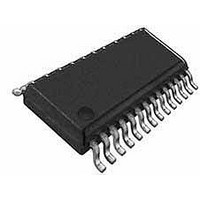
SSOP-28
Minimum Operating Temperature
- 25 C
Lead Free Status / RoHS Status
Lead free / RoHS Compliant
Available stocks
Company
Part Number
Manufacturer
Quantity
Price

Part Number:
WM8510GEDS/RV
Manufacturer:
WOLFSON
Quantity:
20 000


WM8510
POWER SUPPLIES
w
The WM8510 can use up to four separate power supplies:
AVDD and AGND: Analogue supply, powers all analogue functions except the speaker output and
mono output drivers. AVDD can range from 2.5V to 3.6V and has the most significant impact on
overall power consumption (except for power consumed in the headphone). A large AVDD slightly
improves audio quality.
SPKVDD and SPKGND: Headphone and Speaker supplies, power the speaker and mono output
drivers. SPKVDD can range from 2.5V to 5.5V. SPKVDD can be tied to AVDD, but it requires
separate layout and decoupling capacitors to curb harmonic distortion. With a larger SPKVDD, louder
headphone and speaker outputs can be achieved with lower distortion. If SPKVDD is lower than
AVDD (or 1.5 x AVDD for BOOST mode), the output signal may be clipped.
DCVDD: Digital core supply, powers all digital functions except the audio and control interfaces.
DCVDD can range from 1.71V to 3.6V, and has no effect on audio quality. The return path for
DCVDD is DGND, which is shared with DBVDD.
DCVDD should be greater than or equal to 1.9V when using the PLL.
DBVDD can range from 1.71V to 3.6V. DBVDD return path is through DGND.
It is possible to use the same supply voltage for all four supplies. However, digital and analogue
supplies should be routed and decoupled separately on the PCB to keep digital switching noise out of
the analogue signal paths.
Note:
DCVDD should be greater than or equal to 1.9V when using the PLL.
RECOMMENDED POWER UP/DOWN SEQUENCE
In order to minimise output pop and click noise, it is recommended that the WM8510 device is
powered up and down using one of the following sequences:
Power Up When NOT Using the Output 1.5x Boost Stage:
1.
2.
3.
4.
5.
6.
7.
Power Up When Using the Output 1.5x Boost Stage:
1.
2.
3.
4.
5.
6.
7.
8.
Turn on external power supplies. Wait for supply voltage to settle.
Set BIASEN = 1, BUFIOEN = 1 and also the VMIDSEL[1:0] bits in the Power Management
1 register. * Notes 1 and 2.
Wait for the VMID supply to settle. * Note 2.
Enable DAC by setting DACEN = 1.
Enable mixers as required.
Enable output stages as required.
Unmute DAC by setting DACMU = 0.
Turn on external power supplies. Wait for supply voltage to settle.
Enable 1.5x output boost. Set MONOBOOST = 1 and SPKBOOST = 1 as required.
Set BIASEN = 1, BUFIOEN = 1, BUFDCOPEN = 1 and also the VMIDSEL[1:0] bits in the
Power Management 1 register. * Notes 1 and 2.
Wait for the VMID supply to settle. * Note 2.
Enable DAC by setting DACEN = 1.
Enable mixers as required.
Enable output stages as required.
Unmute DAC by setting DACMU = 0.
PD, Rev 4.5 ,September 2008
Production Data
58
Related parts for WM8510GEDS/RV
Image
Part Number
Description
Manufacturer
Datasheet
Request
R

Part Number:
Description:
Manufacturer:
Wolfson Microelectronics
Datasheet: