ASD5010L1000INT Arctic Silicon Devices, ASD5010L1000INT Datasheet
ASD5010L1000INT
Specifications of ASD5010L1000INT


Related parts for ASD5010L1000INT


ASD5010L1000INT Summary of contents
Page 1
Preliminary Product Specification ASD5010 Multi-Mode 8-bit 1000/500/250 MSPS Analog to Digital Converter with Digital Gain Features 8-bit Single/ Dual/ Quad ADC ● 1 Channel Mode: F ● Smax 2 Channel Mode: F ● Smax 4 Channel Mode: F ● Smax ...
Page 2
Preliminary Product Specification Table of Contents Blizzard Product family: Products and Relations..................................................................................................................3 Specifications........................................................................................................................................................................ 4 ASD5010L1000............................................................................................................................................................... 5 ASD5010L500................................................................................................................................................................. 7 Digital and Switching Specifications...................................................................................................................................... 8 Absolute Maximum Ratings.................................................................................................................................................. 9 Pin Configuration and Description....................................................................................................................................... 10 Start up Initialization............................................................................................................................................................ 12 Serial Interface.................................................................................................................................................................... 12 Timing ...
Page 3
Preliminary Product Specification Blizzard Product family: Products and Relations ASD5010 is a part of the ASD Blizzard family of ADCs for Instrumentation applications. The Blizzard family also includes ASD5020 with two main modes High Speed Mode (ASD5020HS): 12-bit up to ...
Page 4
Preliminary Product Specification Specifications AVDD=1.8V, DVDD=1.8V, OVDD=1.8V 100 MSPS, Quad Channel Mode, 50% clock duty cycle, -1dBFS 8 MHz input signal, 1x/0dB digital gain (fine and coarse), unless otherwise noted Parameter DC accuracy No missing codes Offset Offset ...
Page 5
Preliminary Product Specification ASD5010L1000 AVDD=1.8V, DVDD=1.8V, OVDD=1.8V, 50% clock duty cycle, -1dBFS 71 MHz input signal, Gain = 1X, RSDS output data levels unless otherwise noted Parameter Performance SNR Signal to Noise Ratio, excluding interleaving spurs Single Ch Mode , ...
Page 6
Preliminary Product Specification Parameter I Digital and output driver Supply Current DVDD P Analog Power AVDD P Digital Power DVDD P Total Power Dissipation TOT P Power Down Mode dissipation PD P Deep sleep Mode power dissipation SLP P Power ...
Page 7
Preliminary Product Specification ASD5010L500 AVDD=1.8V, DVDD=1.8V, OVDD=1.8V, 50% clock duty cycle, -1dBFS 70 MHz input signal, Gain = 1X, ADC current scaling -40%, RSDS output data levels unless otherwise noted Parameter Description Performance SNR Signal to Noise Ratio, excluding interleaving ...
Page 8
Preliminary Product Specification Digital and Switching Specifications AVDD=1.8V, DVDD=1.8V, OVDD=1.8V, RSDS output data levels, unless otherwise noted Parameter Clock Inputs DC Duty Cycle Compliance V Differential input voltage swing CK,diff V Differential input voltage swing, sine wave clock input CK,sine ...
Page 9
Preliminary Product Specification Absolute Maximum Ratings Applying voltages to the pins beyond those specified in Table 1 could cause permanent damage to the circuit. Pin AVDD DVDD OVDD AVSS / DVSS Analog inputs and outputs CLKx LVDS outputs Digital inputs ...
Page 10
Preliminary Product Specification Pin Configuration and Description AVDD 1 CSN 2 SDATA 3 4 SCLK RESETN DVDD 7 DVSS 8 9 DP1A DN1A 10 DP1B 11 DN1B 12 PIN NAME AVDD Analog power supply, 1.8V CSN Chip ...
Page 11
Preliminary Product Specification PIN NAME DP2B LVDS channel 2B, positive output DN2B LVDS channel 2B, negative output LCKP LVDS bit clock, positive output LCKN LVDS bit clock, negative output FCLKP LVDS frame clock (1X), positive output FCLKN LVDS frame clock ...
Page 12
Preliminary Product Specification Start up Initialization As part of the ASD5010 power-on sequence both a reset and a power down cycle have to be applied to ensure correct start-up initialization. Reset can be done in one of two ways: 1. ...
Page 13
Preliminary Product Specification Timing Diagrams Analog input Input clock LCLK P LCLK N FCLK P FCLK DxnA N-4 N-4 N-4 N-4 N-4 N DxnB N-3 N-3 N-3 N-3 N-3 N-3 Analog input Input clock LCLK ...
Page 14
Preliminary Product Specification Analog input Input clock LCLK P LCLK N FCLK P FCLK Dx1A N-16 N-16 N-16 N-16 N-16 N- Dx1B N-15 N-15 N-15 N-15 N-15 N- Dx2A N-14 N-14 N-14 N-14 ...
Page 15
Preliminary Product Specification Register Map Name Description rst * Self-clearing software reset. sleep4_ch<4:1> Channel-specific sleep mode for a Quad Channel setup. sleep2_ch<2:1> Channel-specific sleep mode for a Dual Channel setup. sleep1_ch1 Channel-specific sleep mode for a Single Channel setup. sleep ...
Page 16
Preliminary Product Specification Name Description in a Dual Channel setup. cgain1_ch1 <3:0> Programmable coarse gain channel Single Channel setup. jitter_ctrl<7:0> Clock jitter adjustment. channel_num <2:0> Set number of channels channels. clk_divide<1:0>* Define ...
Page 17
Preliminary Product Specification Register Description Software Reset Name Description rst Self-clearing software reset. Setting the rst register bit to '1', restores the default value of all the internal registers including the rst register bit itself. Modes of Operation and Clock ...
Page 18
Preliminary Product Specification Input Select Name Description inp_sel_adc1<4:0> Input select for adc 1. inp_sel_adc2<4:0> Input select for adc 2. inp_sel_adc3<4:0> Input select for adc 3. inp_sel_adc4<4:0> Input select for adc 4. Each ADC is connected to the four input signals ...
Page 19
Preliminary Product Specification Full-scale Control Name Description fs_cntrl<5:0> Fine adjust ADC full scale range The full-scale voltage range of ASD5010 can be adjusted using an internal 6-bit DAC controlled by the fs_cntrl register. Changing the value in the register by ...
Page 20
Preliminary Product Specification The ext_vcm_bc register controls the driving strength in the buffer supplying the voltage on the VCM pin. If this pin is not in use, the buffer can be switched off. If current is drawn from the VCM ...
Page 21
Preliminary Product Specification Start-up and Clock Jitter Control Name Description startup_ctrl<2:0> Controls start-up time. jitter_ctrl<7:0> Clock jitter adjustment. To optimize start up time, a register is provided where the start-up time in number of clock cycles can be set. Some ...
Page 22
Preliminary Product Specification Number of bits to '1' in jitter_ctrl<7:0> ASD5010 Table 13: Clock jitter performance Clock jitter performance Module current consumption [fsrms] 160 150 136 130 126 124 122 120 ...
Page 23
Preliminary Product Specification LVDS Output Configuration and Control Name Description low_clk_freq Low clock frequency used. lvds_advance Advance LVDS data bits and frame clock by one clock cycle lvds_delay Delay LVDS data bits and frame clock by one clock cycle phase_ddr<1:0> ...
Page 24
Preliminary Product Specification Mode of operation Single channel Dual channel Quad channel To ease timing in the receiver when using multiple ASD5010, the device has the option to adjust the timing of the output data and the frame clock. The ...
Page 25
Preliminary Product Specification The default data output format is offset binary. Two's complement mode can be selected by setting the btc_mode bit to '1' which inverts the MSB. The first bit of the frame (following the rising edge of FCLKP) ...
Page 26
Preliminary Product Specification PCB traces. This may result in reflections back to the LVDS outputs and loss of signal integrity. This effect can be mitigated by enabling an internal termination between the positive and negative outputs of each LVDS buffer. ...
Page 27
Preliminary Product Specification Power Mode Control Name Description sleep4_ch<4:1> Channel-specific sleep mode for a Quad Channel setup. sleep2_ch<2:1> Channel-specific sleep mode for a Dual Channel setup. sleep1_ch1 Channel-specific sleep mode for a Single Channel setup. sleep Go to sleep-mode. pd ...
Page 28
Preliminary Product Specification Programmable Gain Name Description cgain_cfg Configures the coarse gain setting fine_gain_en Enable use of fine gain. cgain4_ch1 <3:0> Programmable coarse gain channel Quad Channel setup. cgain4_ch2 <3:0> Programmable coarse gain channel ...
Page 29
Preliminary Product Specification cgain_cfg There is a digital fine gain implemented for each ADC to adjust the fine gain errors between the ADCs. The gain is controlled by fgain_branch* as defined in table 22. There will be no missing codes ...
Page 30
Preliminary Product Specification Analog Input Invert Name Description invert4_ch<4:1> Channel specific swapping of the analog input signal for a Quad Channel setup. invert2_ch<2:1> Channel specific swapping of the analog input signal for a Dual Channel setup. invert1_ch1 Channel specific swapping ...
Page 31
Preliminary Product Specification Theory of Operation ASD5010 is a multi Mode high-speed, CMOS ADC, consisting of 8 ADC branches, configured in different channel modes, using interleaving to achieve high speed sampling. For all practical purposes, the device can be considered ...
Page 32
Preliminary Product Specification side of the resistors may be used to provide dynamic charging currents and may improve performance. The resistors form a low pass filter with the capacitor, and values must therefore be determined by requirements for the application. ...
Page 33
Preliminary Product Specification all circuitry in the clock distribution utmost importance to avoid crosstalk between the ADC output bits and the clock and between the analog input signal and the clock since such crosstalk often results in ...
Page 34
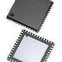
Preliminary Product Specification Package Mechanical Data QFN48 Pin 1 ID (Top side Symbol Min A 0 5. 0.6 ASD5010 D D2 Pin 1 ID Radius ...
Page 35
... Preliminary Product Specification Ordering information Model Temp. range ASD5010L500INT -40 to +85 °C ASD5010L1000INT -40 to +85 °C (1) MSL, Peak Temp: The moisture sensitivity level rating classified according to the JEDEC industry standard and to peak solder temperature. Datasheet status Objective Product Specification: The values and functionality describe design targets only. Specifications and functionality can be changed without notice. ...