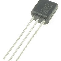
2N5060 Central Semiconductor, 2N5060 Datasheet - Page 3

2N5060
Manufacturer Part Number
2N5060
Description
SCRs 0.8A 30V
Manufacturer
Central Semiconductor
Datasheet
1.2N5060.pdf
(8 pages)
Specifications of 2N5060
Breakover Current Ibo Max
10 A
Rated Repetitive Off-state Voltage Vdrm
30 V
Off-state Leakage Current @ Vdrm Idrm
0.01 mA
Forward Voltage Drop
1.7 V
Gate Trigger Voltage (vgt)
1.2 V
Maximum Gate Peak Inverse Voltage
5 V
Gate Trigger Current (igt)
0.35 mA
Holding Current (ih Max)
10 mA
Mounting Style
Through Hole
Package / Case
TO-92
Lead Free Status / RoHS Status
Lead free / RoHS Compliant
Available stocks
Company
Part Number
Manufacturer
Quantity
Price
Company:
Part Number:
2N5060RLRAG
Manufacturer:
ON
Quantity:
32 000
Company:
Part Number:
2N5060RLRAG
Manufacturer:
ON Semiconductor
Quantity:
1 600
3. R
4. Forward current applied for 1 ms maximum duration, duty cycle p 1%.
5. R
*Indicates JEDEC Registered Data.
ELECTRICAL CHARACTERISTICS
OFF CHARACTERISTICS
ON CHARACTERISTICS
DYNAMIC CHARACTERISTICS
Symbol
V
I
V
I
V
I
*Peak Repetitive Forward or Reverse Blocking Current (Note 3)
*Peak Forward On−State Voltage (Note 4)
Gate Trigger Current (Continuous DC) (Note 5)
Gate Trigger Voltage (Continuous DC) (Note 5)
*Gate Non−Trigger Voltage
Holding Current (Note 5)
Turn-On Time
Turn-Off Time
Critical Rate of Rise of Off−State Voltage
DRM
RRM
H
DRM
RRM
TM
(V
(I
*(V
*(V
*(V
Delay Time
Rise Time
(I
Forward Current = 1.0 A, di/dt = 6.0 A/ms
(Forward Current = 1.0 A pulse,
Pulse Width = 50 ms,
0.1% Duty Cycle, di/dt = 6.0 A/ms,
dv/dt = 20 V/ms, I
(Rated V
(V
GK
GK
TM
GT
AK
AK
AK
AK
AK
= 1000 W is included in measurement.
current is not included in measurement.
= 1.0 mA, V
= 1.2 A peak @ T
= Rated V
= Rated V
= 7.0 Vdc, R
= 7.0 Vdc, R
= 7.0 Vdc, initiating current = 20 mA)
DRM
Parameter
Peak Repetitive Off State Forward Voltage
Peak Forward Blocking Current
Peak Repetitive Off State Reverse Voltage
Peak Reverse Blocking Current
Peak on State Voltage
Holding Current
, Exponential)
DRM
DRM
D
GT
= Rated V
L
L
, R
or V
= 100 W)
= 100 W)
= 1 mA)
A
L
= 25 C)
RRM
= 100 W) T
DRM
)
Characteristic
,
C
Voltage Current Characteristic of SCR
= 110 C
(T
C
2N5060, 2N5061
2N5062, 2N5064
= 25 C unless otherwise noted)
http://onsemi.com
2N5060 Series
T
T
T
T
T
T
T
T
C
C
C
C
C
C
C
C
= 25 C
= 110 C
= 25 C
= −40 C
= 25 C
= −40 C
= 25 C
= −40 C
3
I
Reverse Avalanche Region
Anode −
RRM
Reverse Blocking Region
at V
RRM
(off state)
on state
I
DRM
Symbol
dv/dt
V
V
V
I
GT
I
t
t
, I
TM
GD
t
GT
+ Current
H
d
q
r
RRM
Forward Blocking Region
I
H
Min
0.1
V
−
−
−
−
−
−
−
−
−
−
−
−
−
−
TM
(off state)
Typ
I
3.0
0.2
10
30
30
DRM
−
−
−
−
−
−
−
−
−
−
Anode +
at V
Max
200
350
1.7
0.8
1.2
5.0
10
50
10
DRM
−
−
−
−
−
−
+ Voltage
Unit
V/ms
mA
mA
mA
mA
ms
ms
V
V
V


