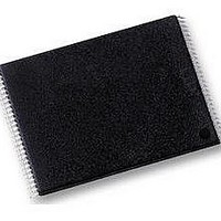
S29GL032N90TFI030 Spansion Inc., S29GL032N90TFI030 Datasheet - Page 48

S29GL032N90TFI030
Manufacturer Part Number
S29GL032N90TFI030
Description
Flash 3V 32Mb Float Gate two address 90s
Manufacturer
Spansion Inc.
Datasheet
1.S29GL032N90TFI010.pdf
(81 pages)
Specifications of S29GL032N90TFI030
Memory Type
NOR
Memory Size
32 Mbit
Access Time
90 ns
Data Bus Width
8 bit, 16 bit
Architecture
Uniform / Boot Sector
Interface Type
Page-mode
Supply Voltage (max)
3.6 V
Supply Voltage (min)
2.7 V
Maximum Operating Current
50 mA
Mounting Style
SMD/SMT
Operating Temperature
+ 85 C
Package / Case
TSOP-48
Ic Interface Type
CFI, Parallel
Supply Voltage Range
2.7V To 3.6V
Memory Case Style
TSOP
No. Of Pins
48
Lead Free Status / RoHS Status
Lead free / RoHS Compliant
Lead Free Status / RoHS Status
Lead free / RoHS Compliant, Lead free / RoHS Compliant
Available stocks
Company
Part Number
Manufacturer
Quantity
Price
Company:
Part Number:
S29GL032N90TFI030
Manufacturer:
SPANSION
Quantity:
6 035
Part Number:
S29GL032N90TFI030
Manufacturer:
SPANSION
Quantity:
20 000
Company:
Part Number:
S29GL032N90TFI030
Manufacturer:
SPANSIO
Quantity:
3 888
Company:
Part Number:
S29GL032N90TFI030H
Manufacturer:
Spansion
Quantity:
1 440
Part Number:
S29GL032N90TFI030H
Manufacturer:
SPANSION
Quantity:
20 000
10.7
48
Sector Erase Command Sequence
Sector erase is a six bus cycle operation. The sector erase command sequence is initiated by writing two
unlock cycles, followed by a set-up command. Two additional unlock cycles are written, and are then followed
by the address of the sector to be erased, and the sector erase command.
Table 10.3 on page 53
The device does not require the system to preprogram prior to erase. The Embedded Erase algorithm
automatically programs and verifies the entire memory for an all zero data pattern prior to electrical erase.
The system is not required to provide any controls or timings during these operations.
After the command sequence is written, a sector erase time-out of 50 µs occurs. During the time-out period,
additional sector addresses and sector erase commands may be written. Loading the sector erase buffer may
be done in any sequence, and the number of sectors may be from one sector to all sectors. The time between
these additional cycles must be less than 50 µs, otherwise erasure may begin. Any sector erase address and
command following the exceeded time-out may or may not be accepted. It is recommended that processor
interrupts be disabled during this time to ensure all commands are accepted. The interrupts can be
re-enabled after the last Sector Erase command is written. Any command other than Sector Erase or
Erase Suspend during the time-out period resets the device to the read mode. Note that the Secured
Silicon Sector, autoselect, and CFI functions are unavailable when an erase operation is in progress.
The system must rewrite the command sequence and any additional addresses and commands.
The system can monitor DQ3 to determine if the sector erase timer has timed out (See the section on DQ3:
Sector Erase Timer.). The time-out begins from the rising edge of the final WE# pulse in the command
sequence.
When the Embedded Erase algorithm is complete, the device returns to reading array data and addresses
are no longer latched. The system can determine the status of the erase operation by reading DQ7, DQ6, or
DQ2 in the erasing sector. Refer to the Write Operation Status section for information on these status bits.
Once the sector erase operation begins, only the Erase Suspend command is valid. All other commands are
ignored. However, note that a hardware reset immediately terminates the erase operation. If that occurs, the
sector erase command sequence should be reinitiated once the device returns to reading array data, to
ensure data integrity.
Figure 10.4 on page 49
parameters, and
Figure 15.7 on page 69
shows the address and data requirements for the sector erase command sequence.
illustrates the algorithm for the erase operation. Refer to
S29GL-N MirrorBit
for timing diagrams.
D a t a
®
Flash Family
S h e e t
Table 10.1 on page 51
S29GL-N_01_12 October 29, 2008
Table 15.3 on page 67
and
for


